Bill and Will's Synth
|
||
Table of Contents |
||
|
This documentation has become so long that we've broken it into three separate pages and sections within them. Here's a table of contents that we hope will make it easier to traverse them: background - presents an explanation and Scott Juskiw's initial description of the module with a photo Parts - presents a Bill of Materials and notes about it Panel - presents the MOTM format panel Mounting Bracket - our home-built custom bracket Construction PCB 1 - MUUB4 Construction PCB 2 - MUUB3 Construction PCB 3 - MUUB3 PCB Connections - wiring the PCBs together Panel Wiring - connecting the PCBs to the panel |
||
Background |
||
|
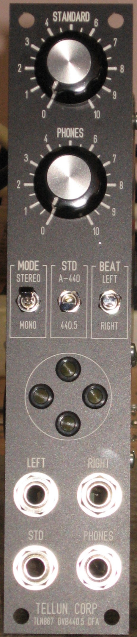
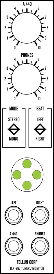
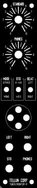
Scott writes: The TLN-867 Tuner & Headphone Monitor combines an A440 reference tone generator, a headphone amplifier, and a beat frequency indicator all in a 1U module. The A440 generator is none other than David Brown's excellent DJB-A440 Reference Oscillator, a super stable digital A440 tone generator. No matter how large your synthesizer is, you don't need more than one A440 tone generator module. A dedicated A440 module would only have a single output jack which, IMHO, is a waste of an entire 1U panel. If, like me, you have just the one head with two ears on it (a mono head), then a headphone monitor is another useful module that you only need one of. Combining the two together makes even more sense should you want to tune your oscillators without sending the A440 tone to your output amp for everyone else to hear. Simply plug your oscillators into the headphone monitor and tune them to the internal A440 tone in complete privacy. The A440 tone has a dedicated volume control so it can be removed from the headphone mix entirely. This is useful for when you want to tune oscillators to some other frequency, or just for having a private mix of any two signals in your synthesizer. The TLN-867 also features a handy beat frequency indicator with four LEDS that provide a visual indication of the frequency difference between the left and right inputs, or either the left or right input with the A440 reference tone. I just like blinky lights, what else can I say? The panel controls are as follows:
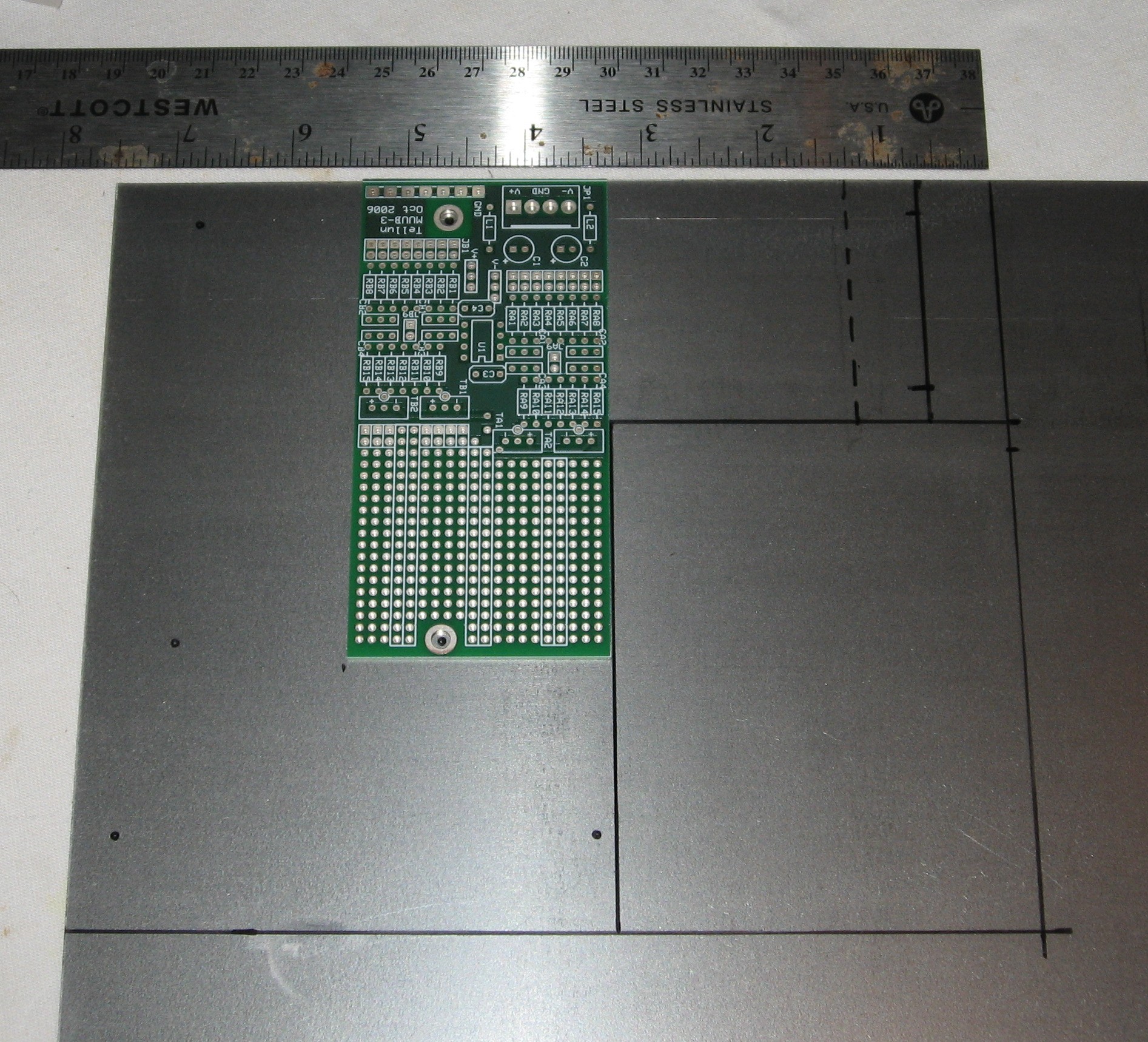
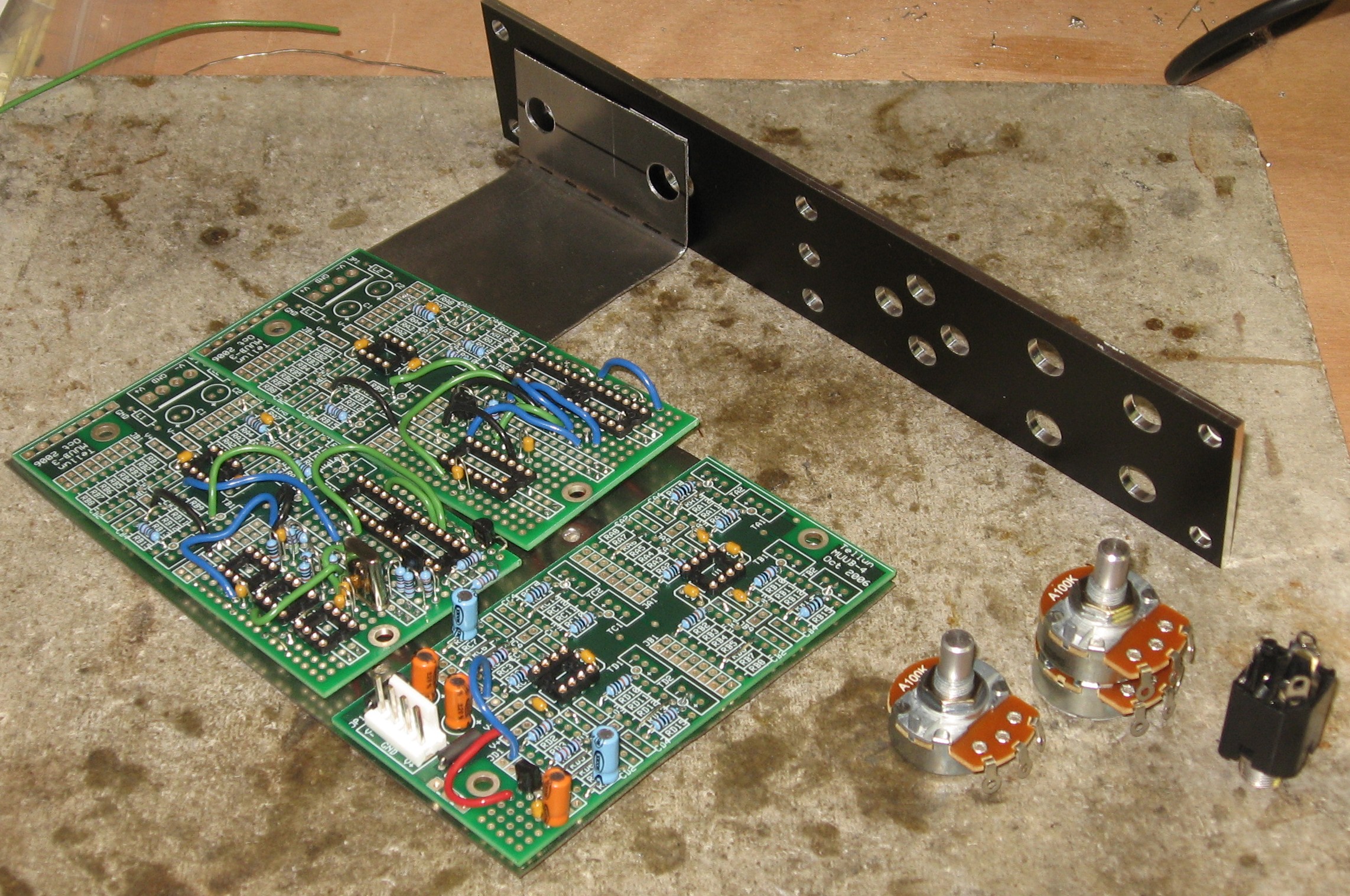
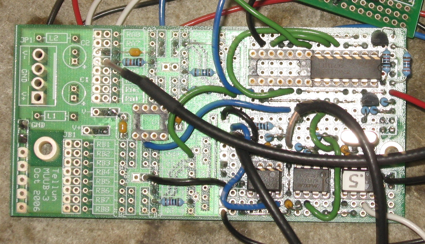
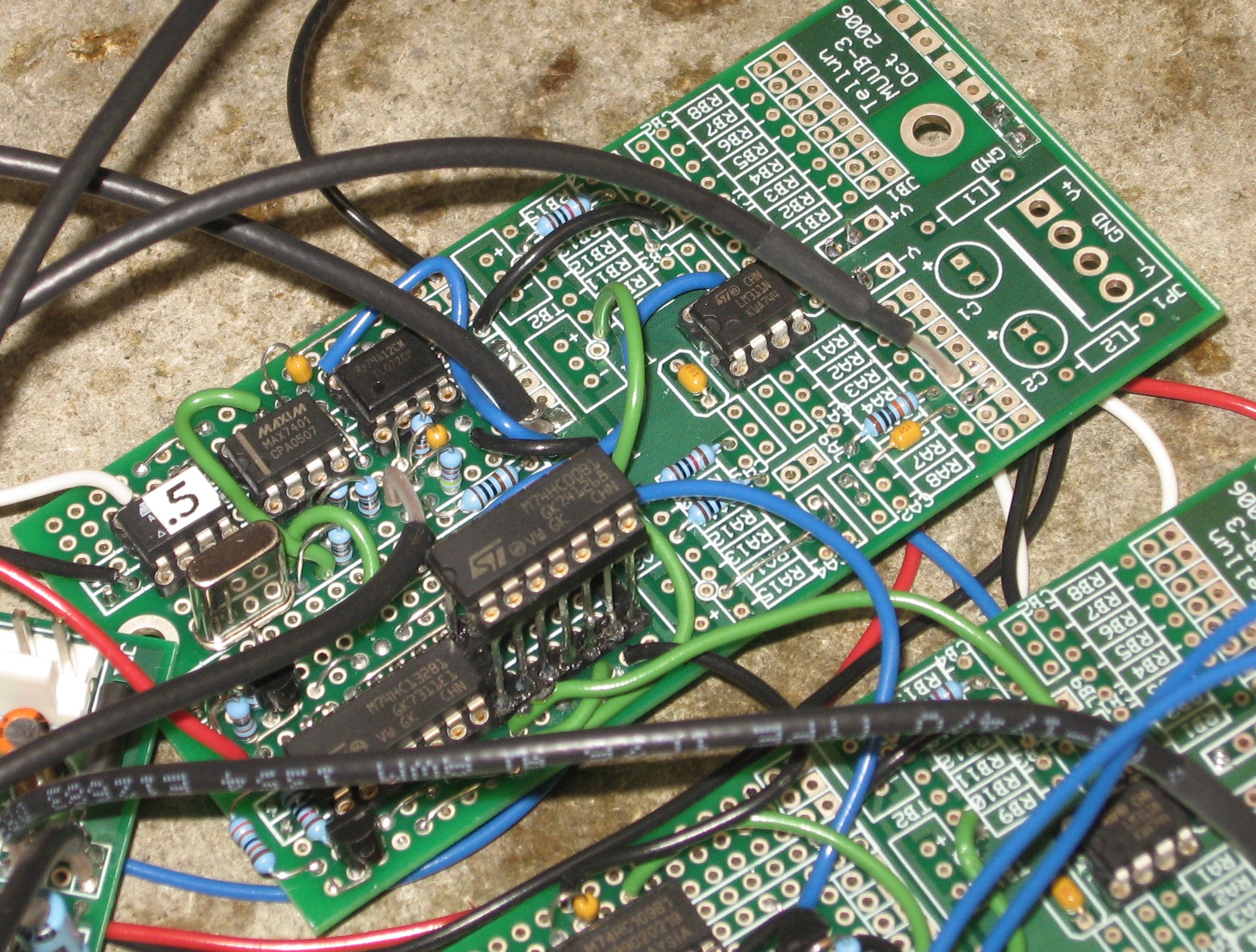
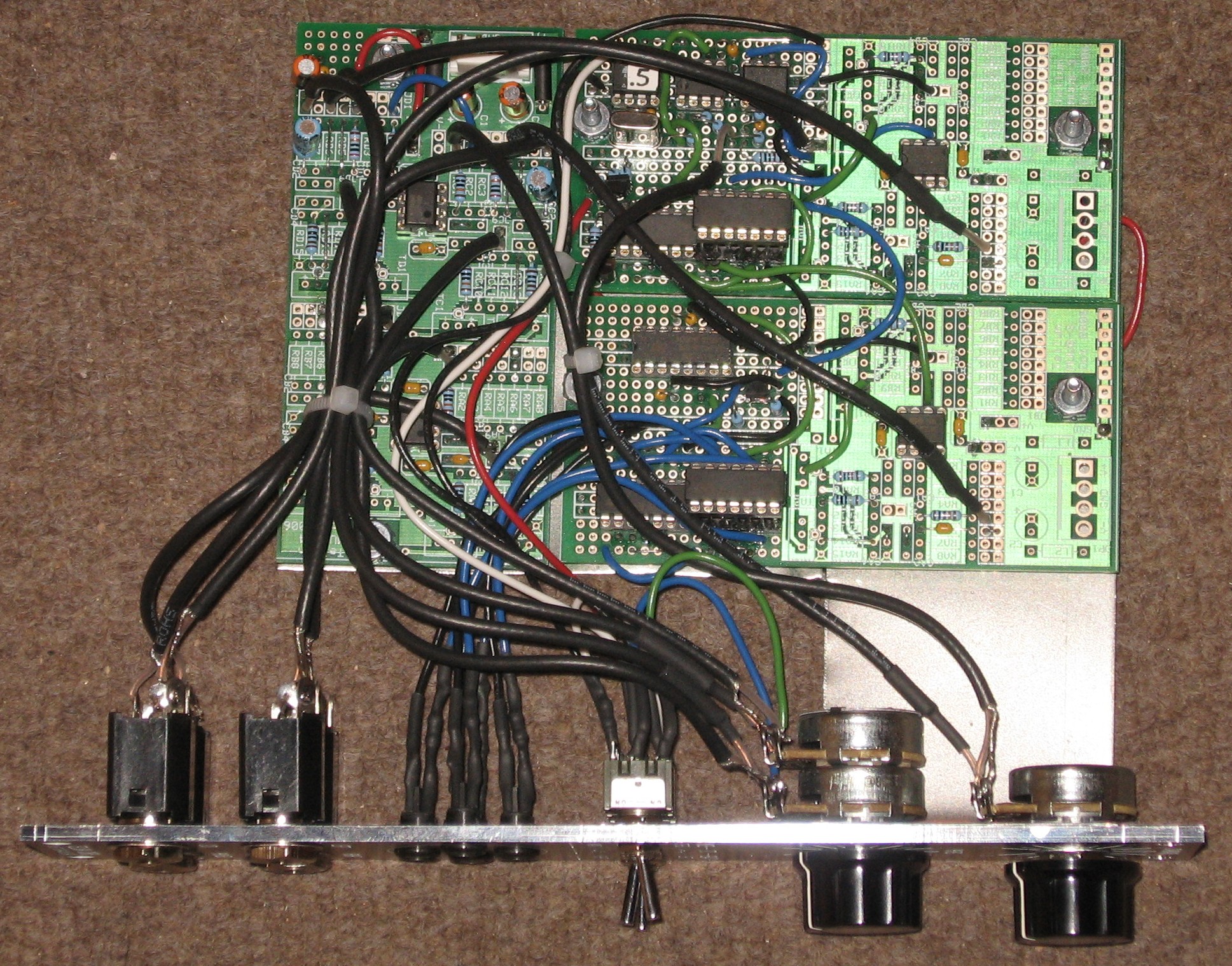
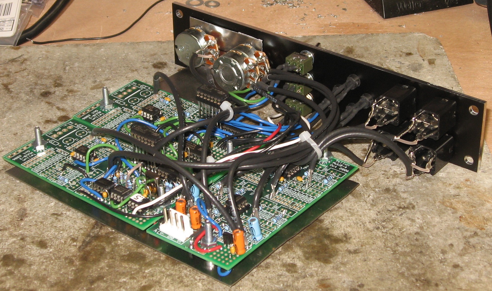
...You’ll need one MUUB-4 and two MUUB-3s to build the TLN-867. If you look at the pictures on the website, you’ll see the three boards mounted on the stooge brackets:
...Total current draw for the TLN-867 is 45 mA @+15V and 27 mA @-15V.
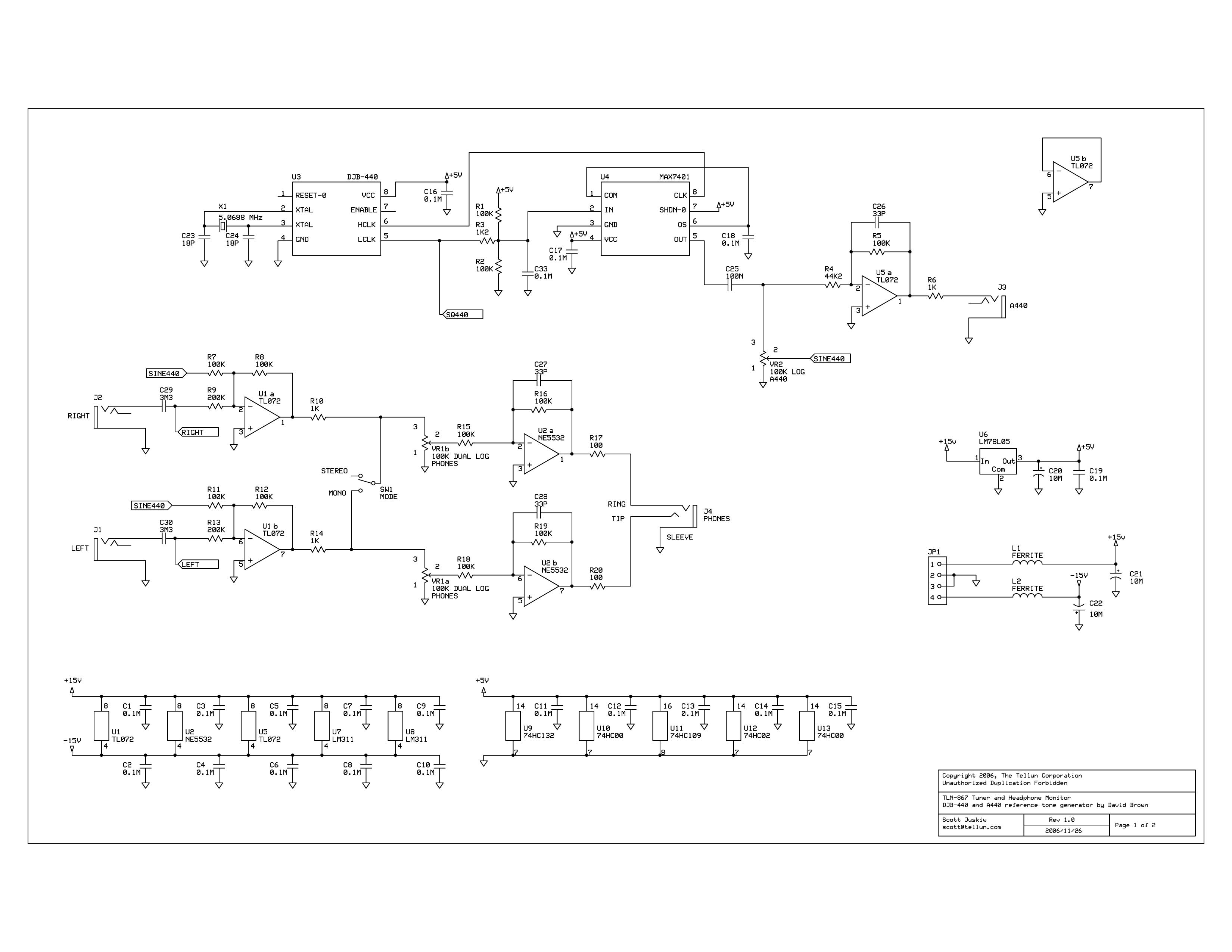
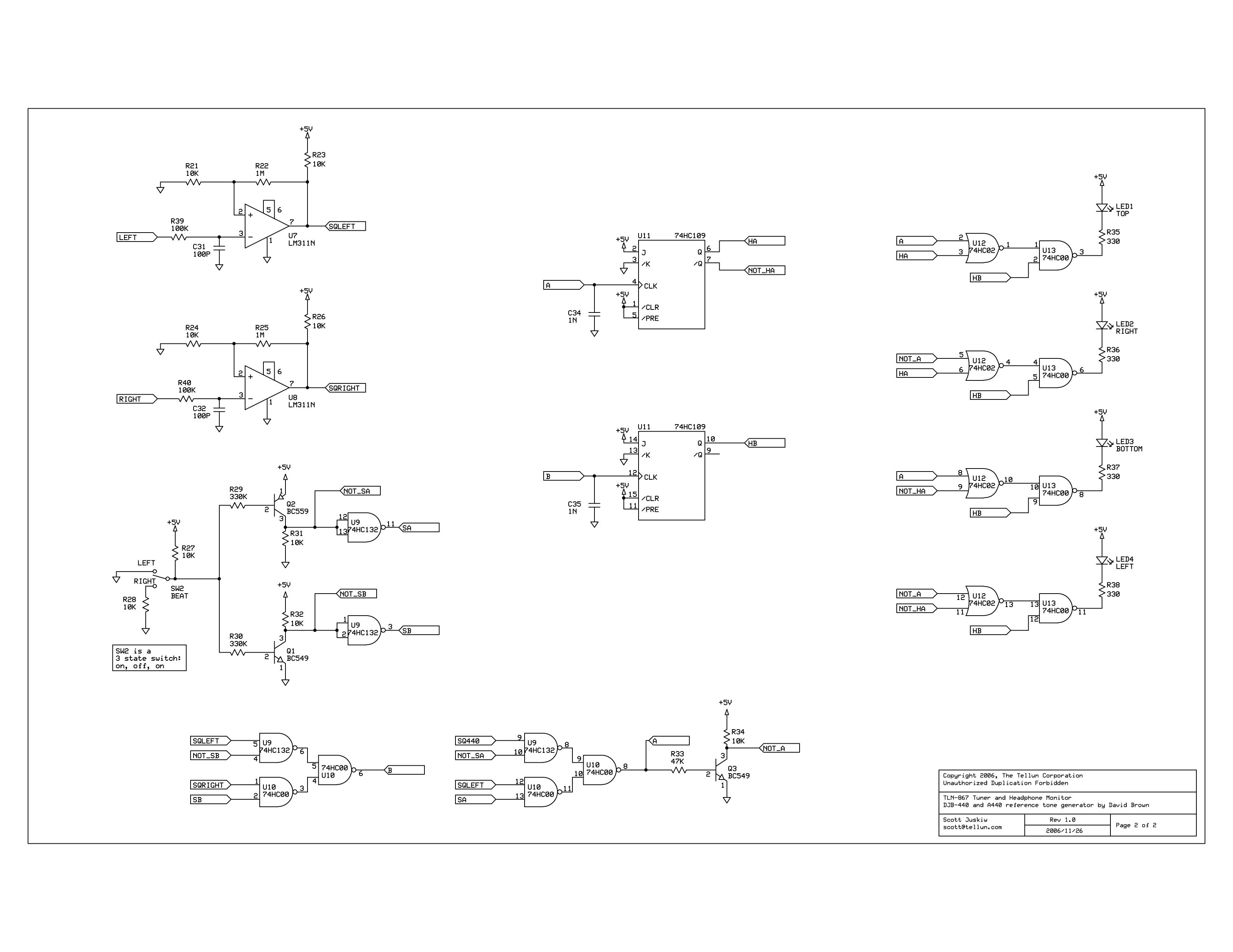
Schematics Here's Scott's Schematics (click on the image to see a high-rez version):
|
||
Modifications |
||
|
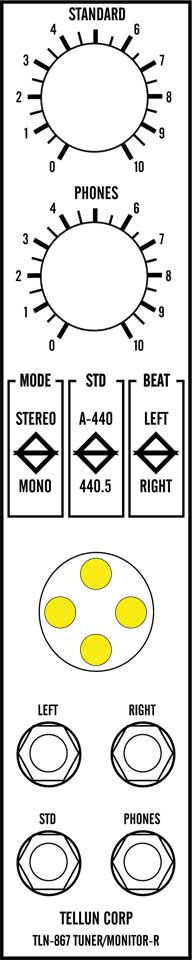
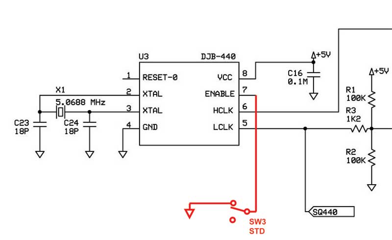
We tune our pianos, guitars, and other acoustic instruments to 440.5 - an average between our non-tunable instruments (Hammond organ is aprox A440.1 and the glockenspiel at aprox 440.8 or 9., etc.) so we asked Dave Brown about the possibility of having a DJB-A440 Reference Oscillator chip made to give a 440.5 reference tone. Even better than we'd hoped, he programmed a chip so it gives both 440 and 440.5 hz outputs - switchable by grounding "pin 7" of the chip. Of this special-made chip, Dave wrote to us:
"Pin 5 is your output at 440 Hz We couldn't have hoped for better. So we'll put an additional switch on the panel to toggle between the two values and we'll adjust some of the labeling accordingly. Here's the modification worked into the schematic diagram - switch up = 440, switch down = 440.5:
|
||
Parts |
||
|
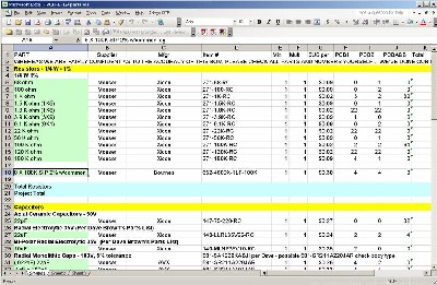
Will and I have developed a parts-list / bill-of-materials in the form of an XL spreadsheet (as usual). We want to thank Dave Brown for making two DJB400s for us one in Feb of 2007 which was the original and the new, modified one that has the 400.5 option. We've used it this parts list to make our Mouser purchases and we are relatively confident in our specifications.
Click here to download our XL spreadsheet Parts List |
||
|
Panel |
||
|
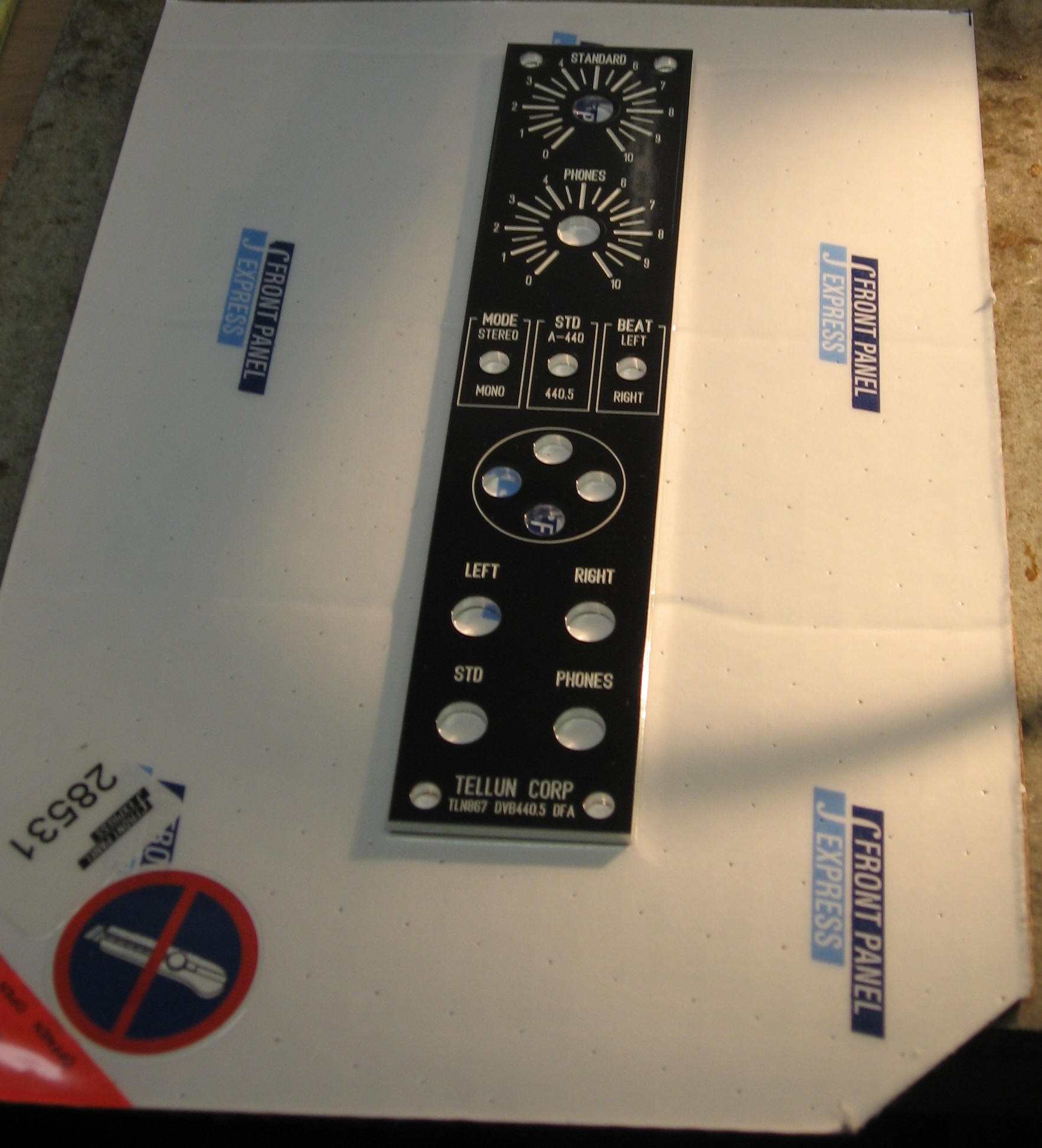
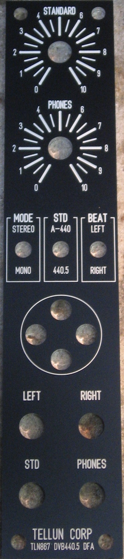
We developed a Front Panel Express panel (FPD) based on Scott Juskiw's design but including the extra switch for the DJB-400 modification. Click on the image below to download the FPD file.
Here's how it came from Front Panel Express:
|
||
|
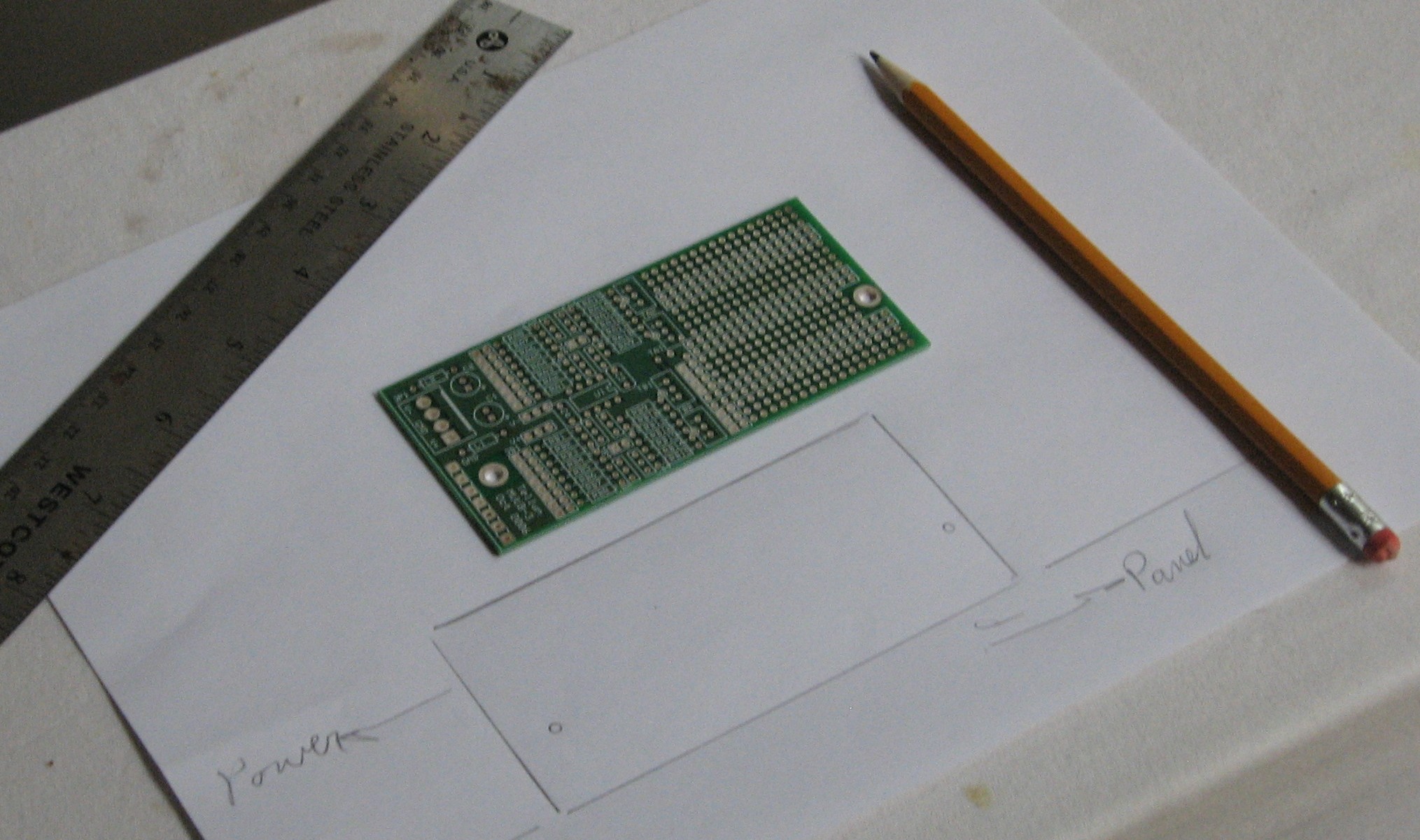
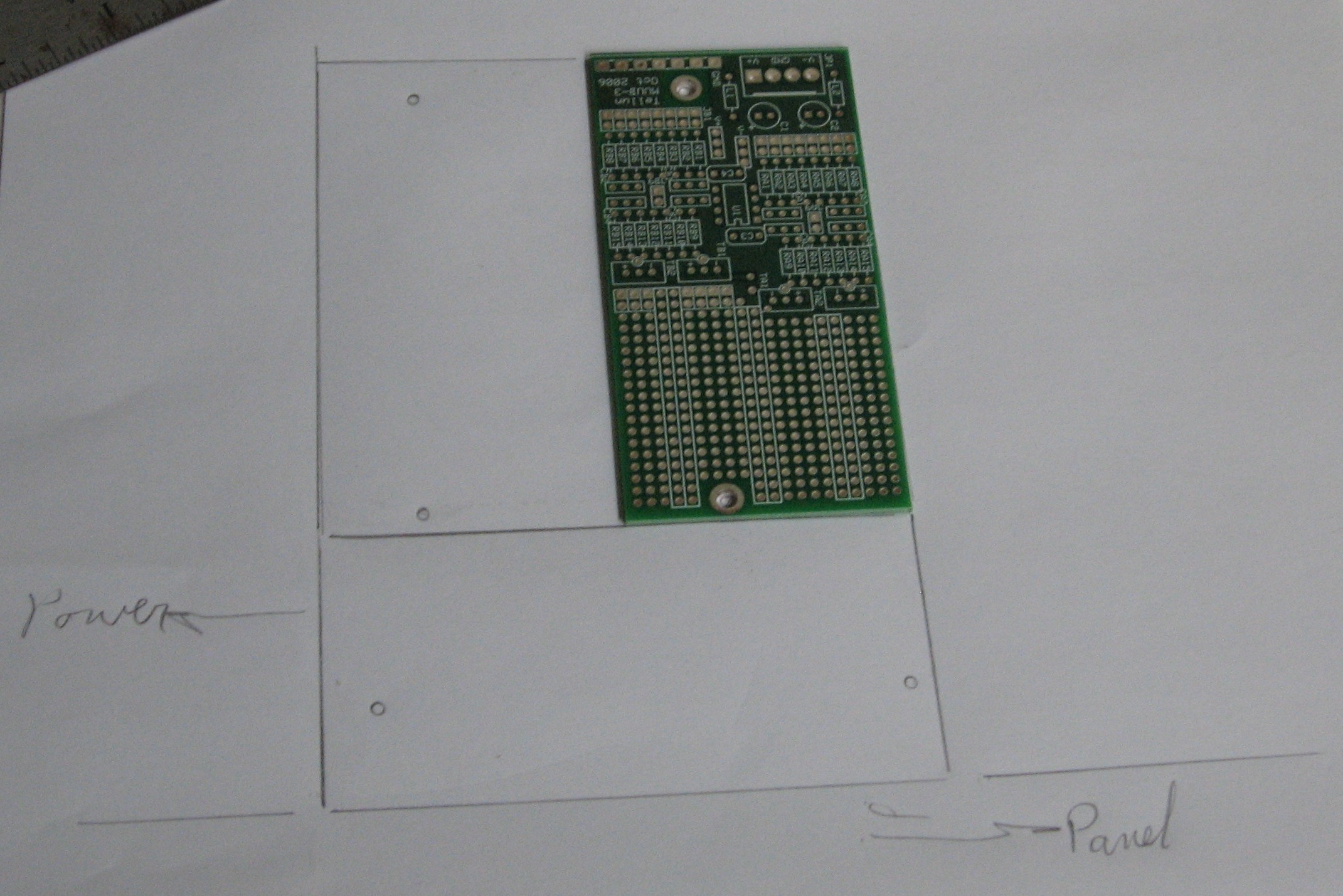
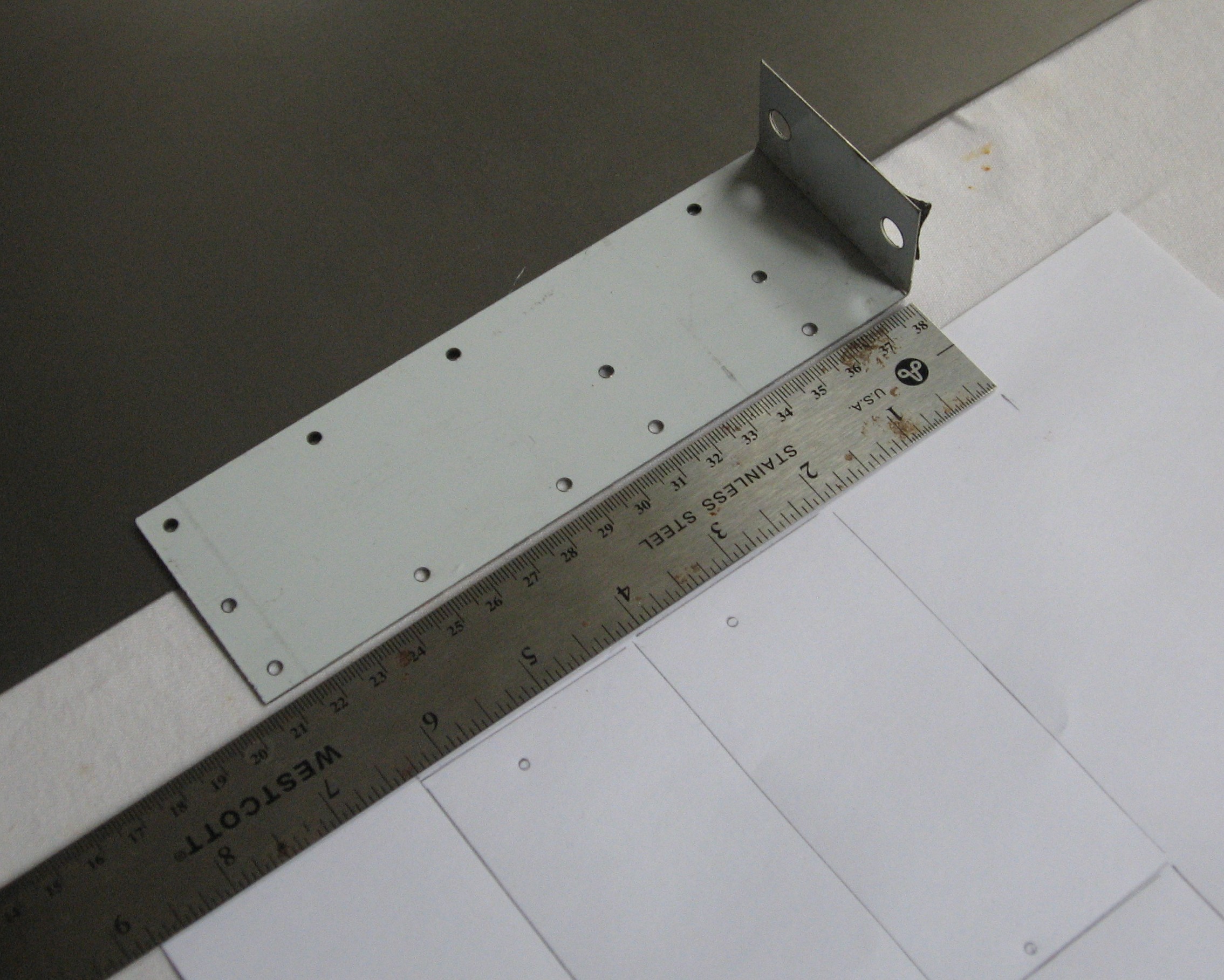
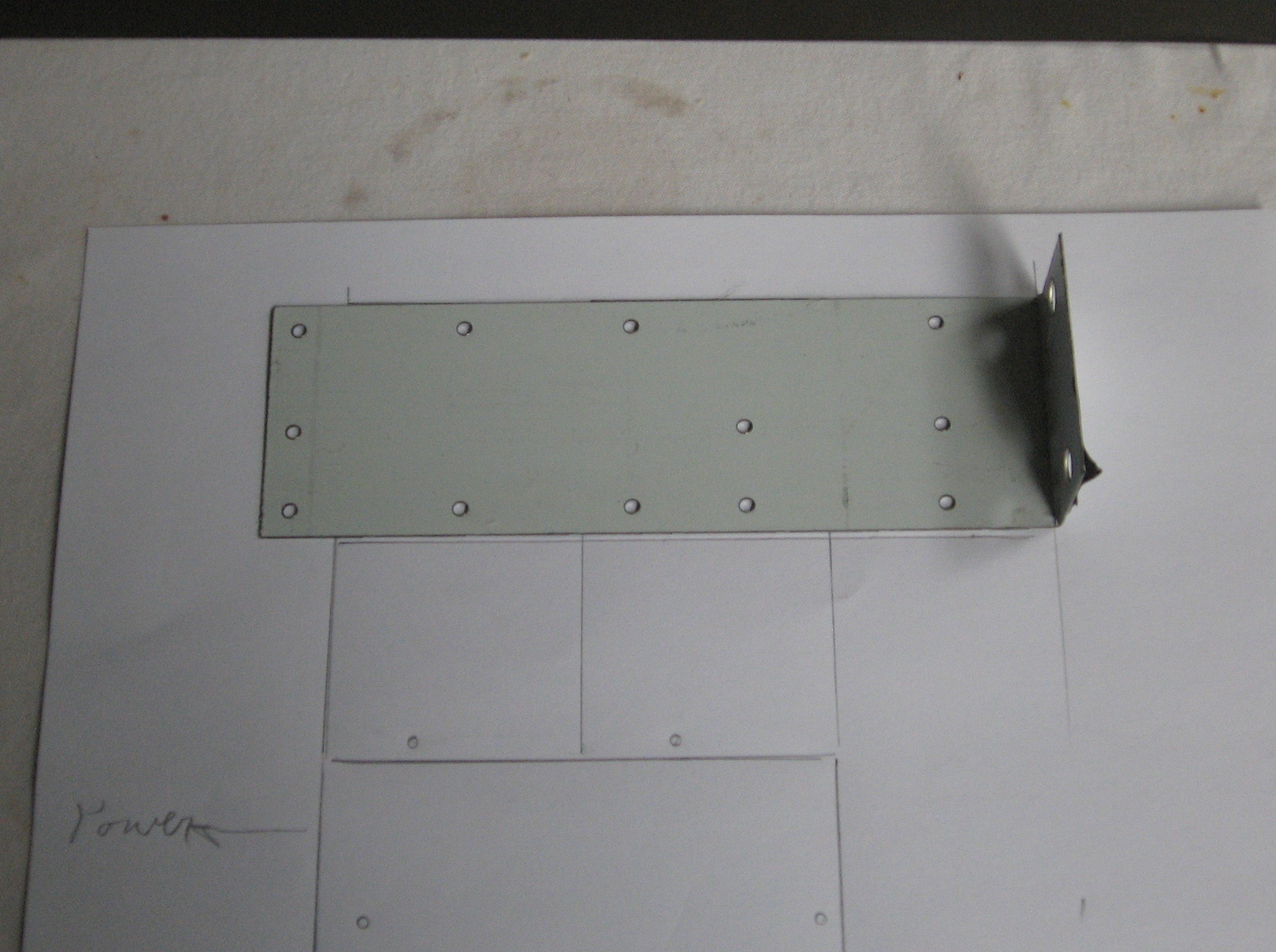
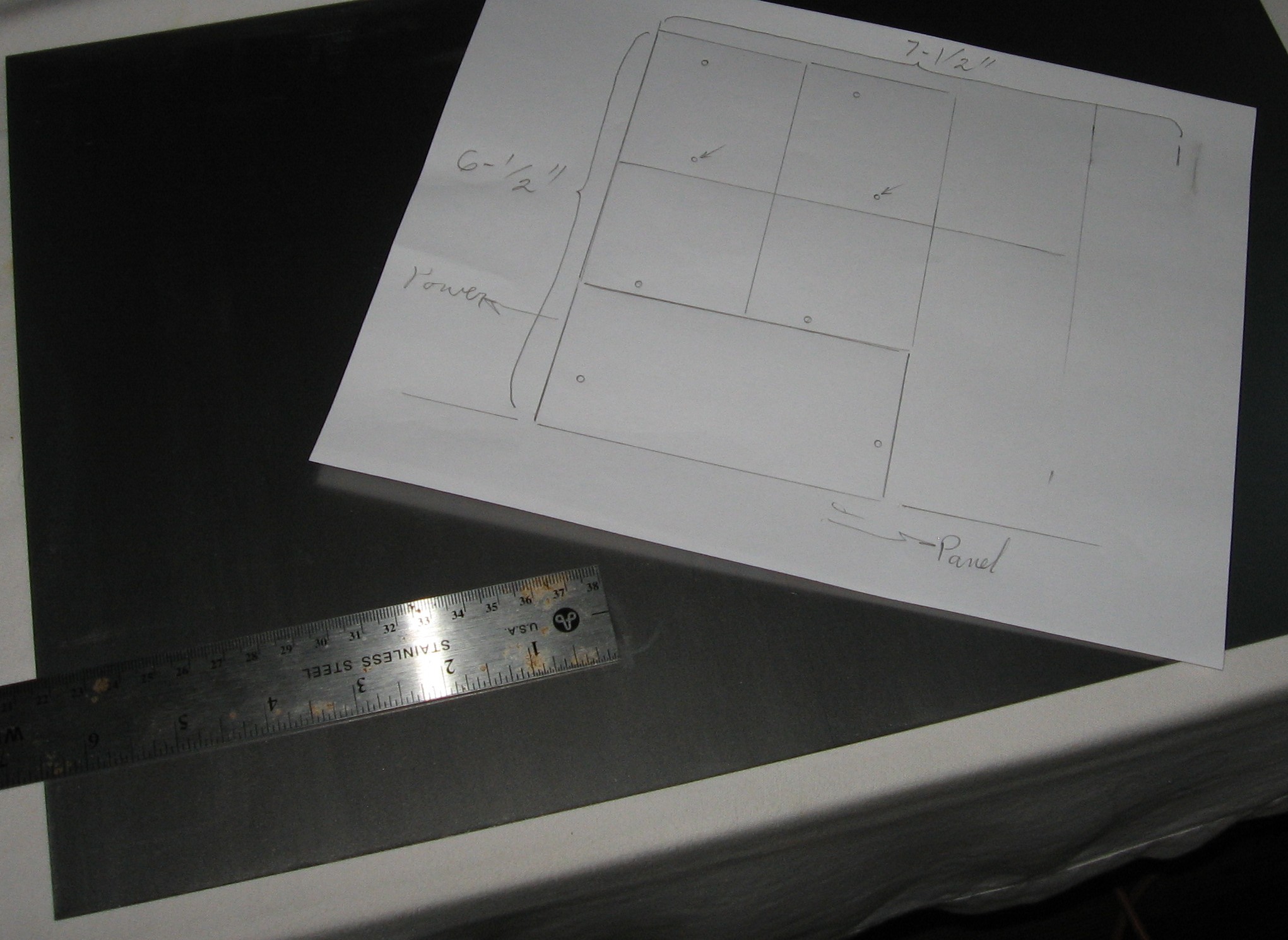
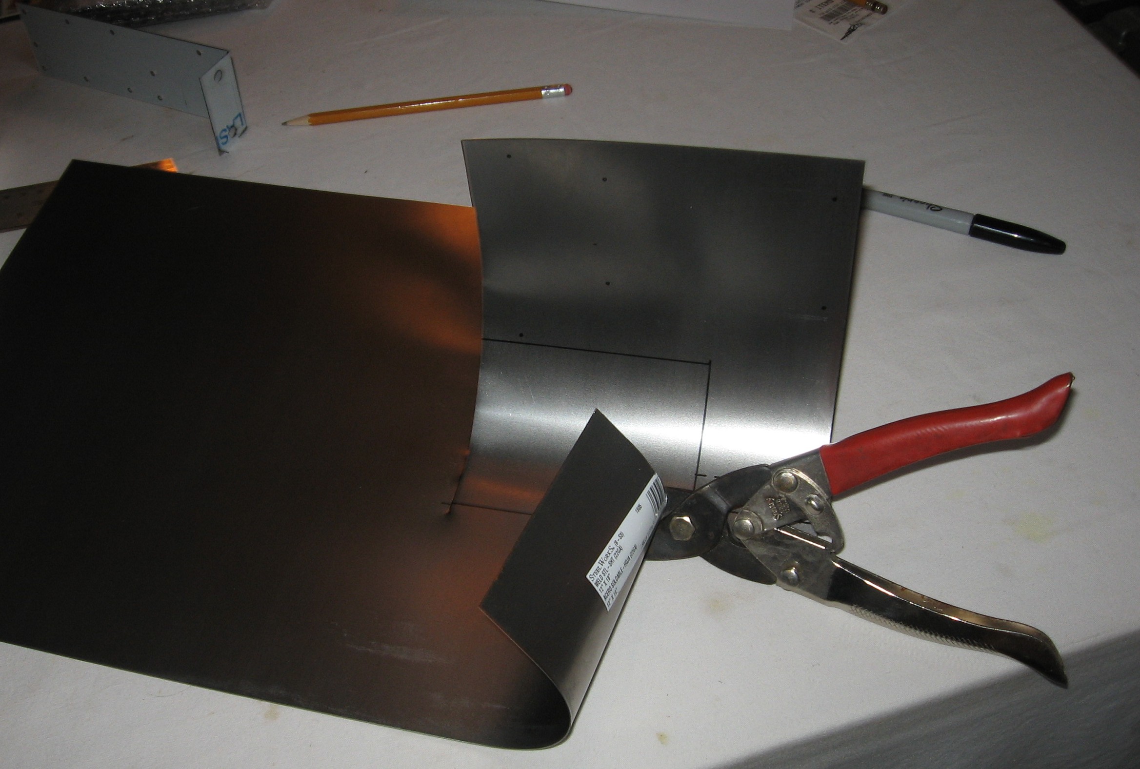
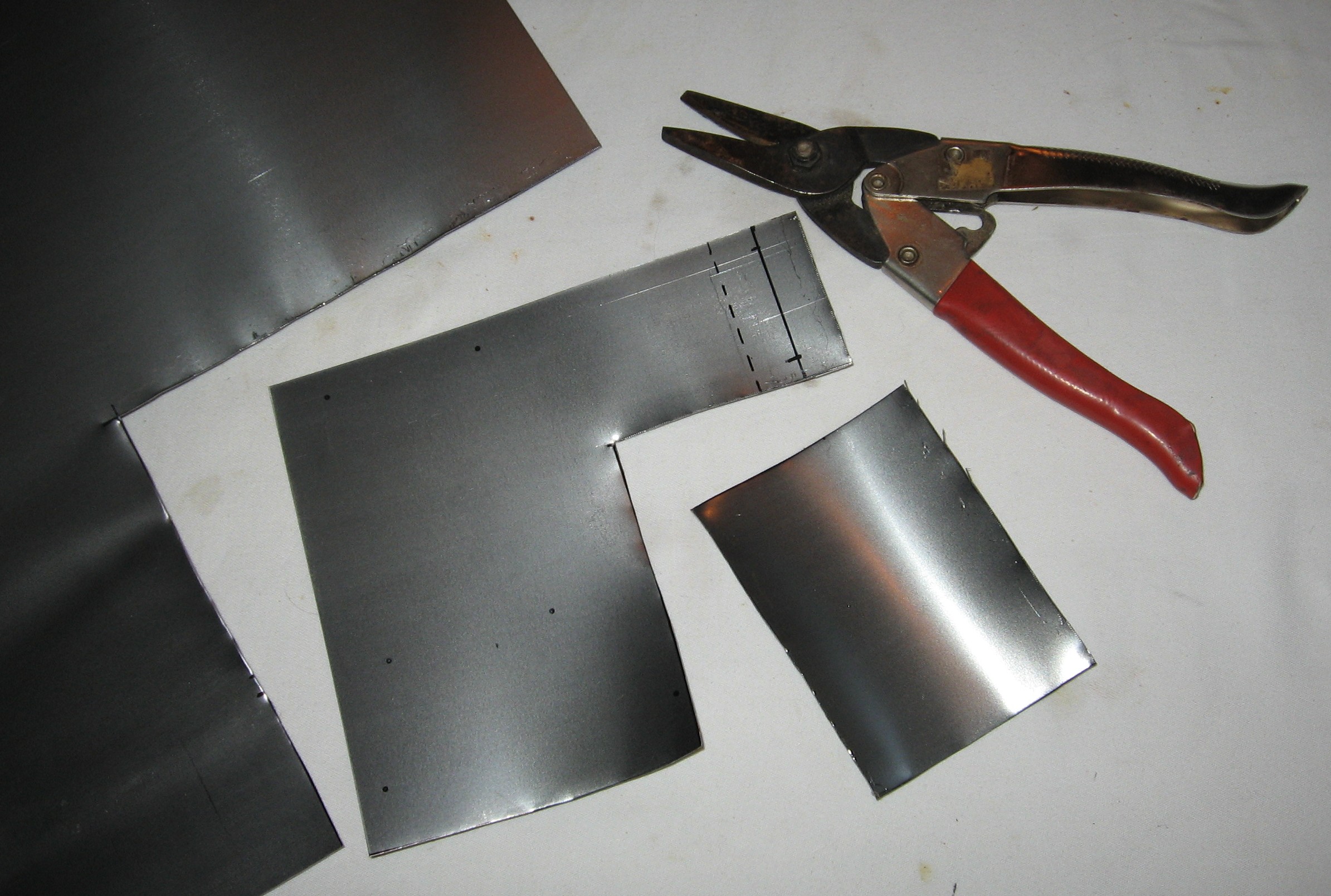
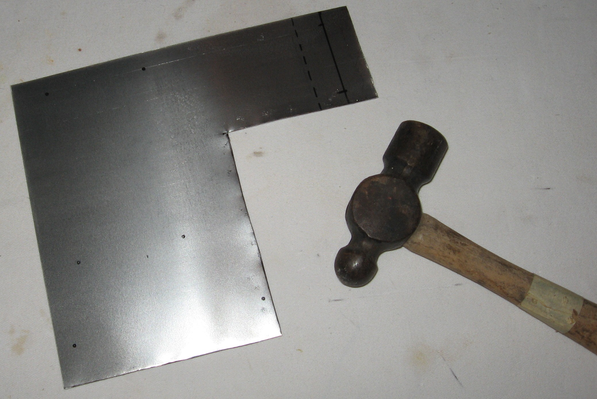
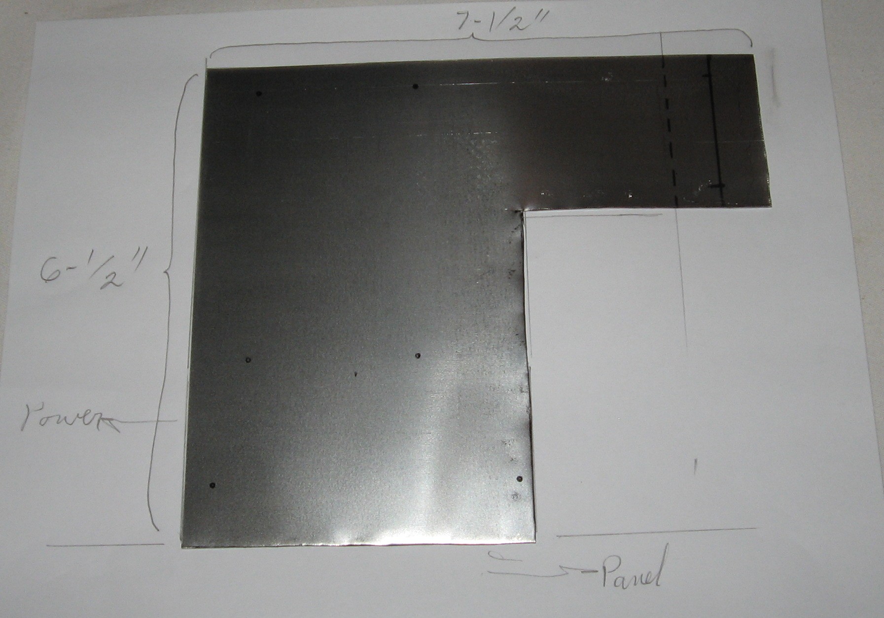
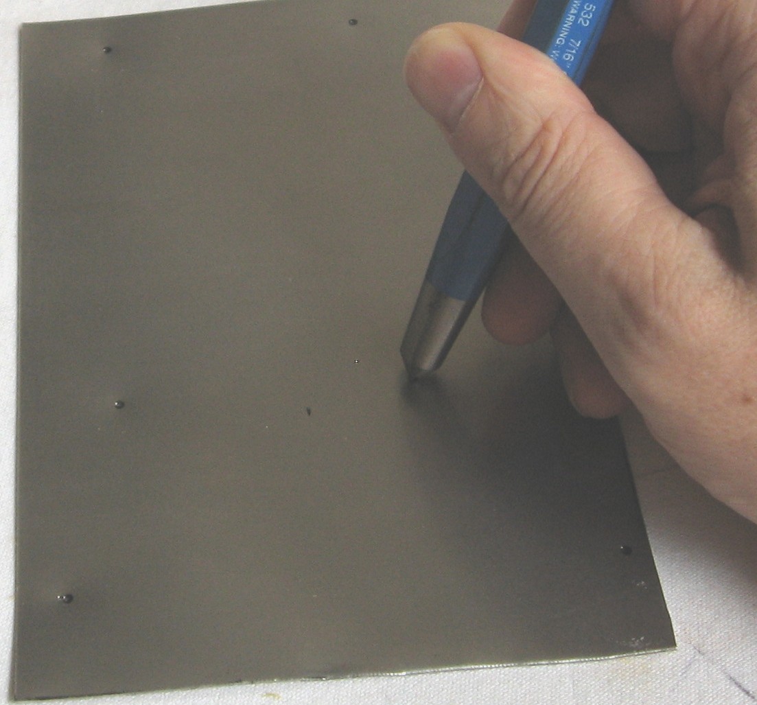
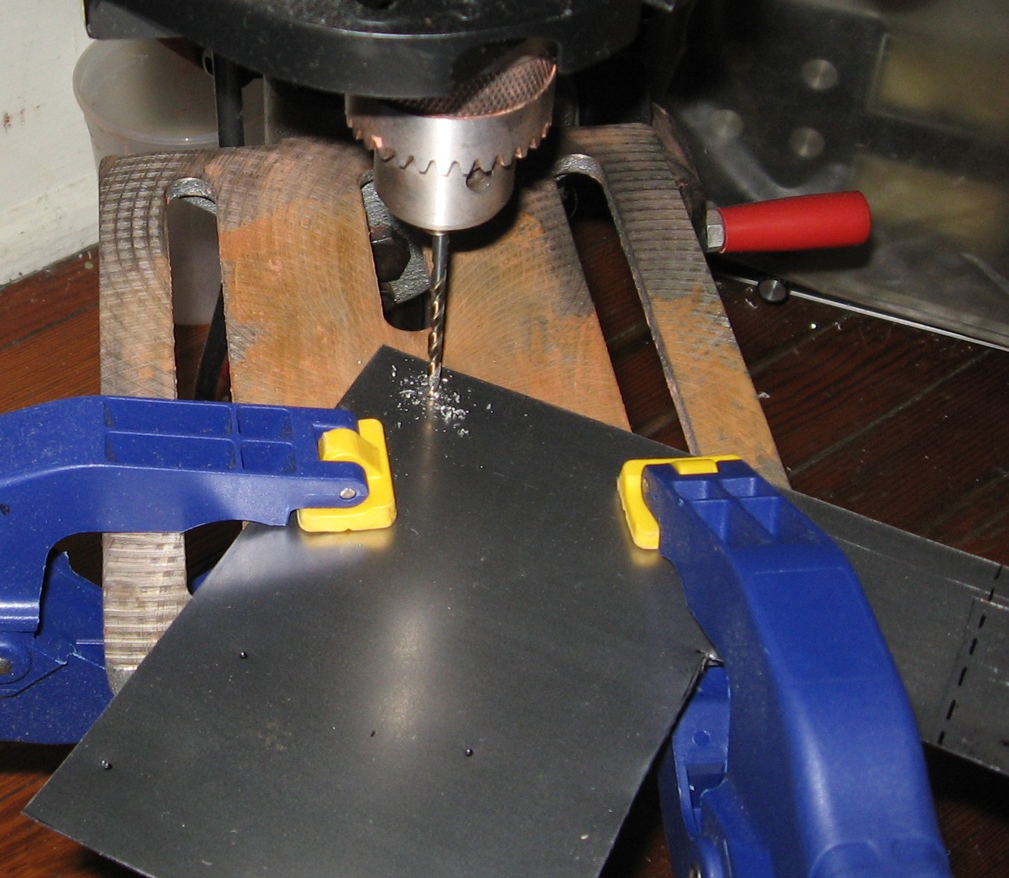
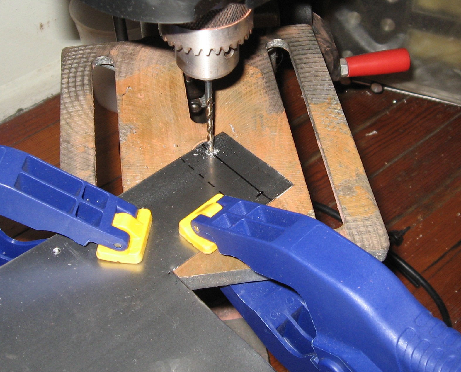
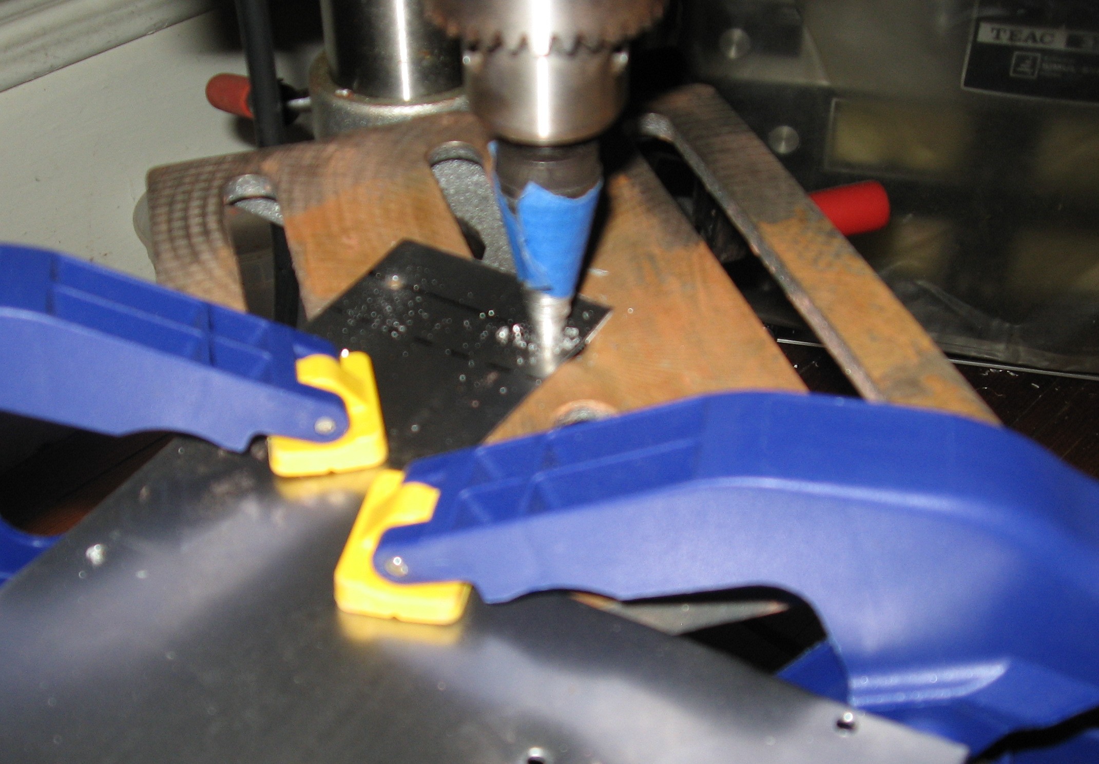
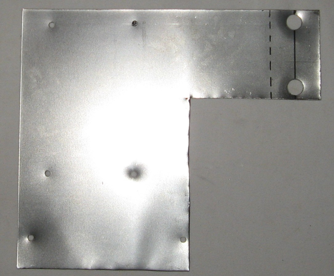
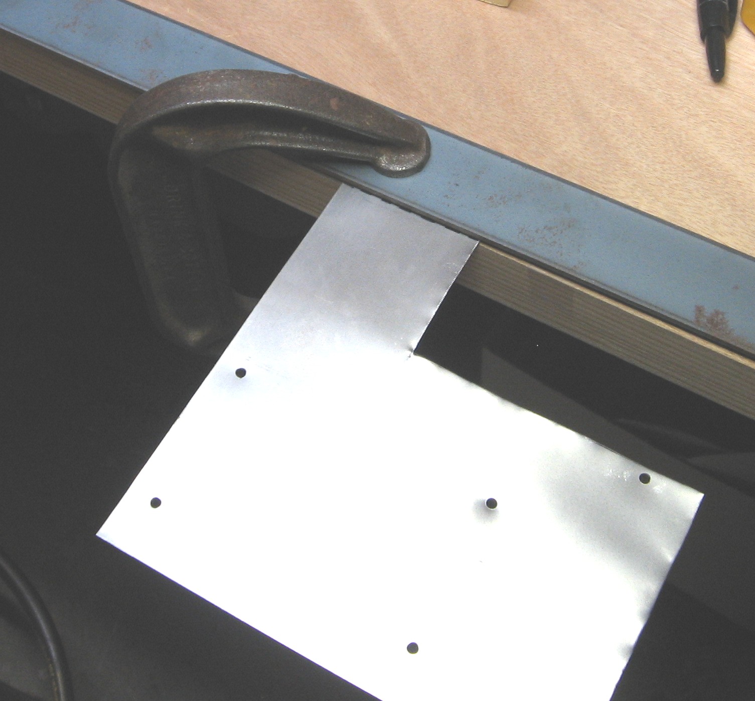
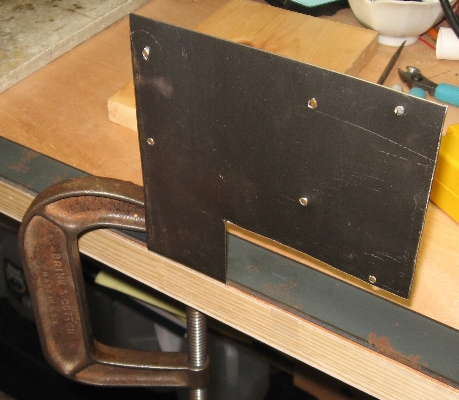
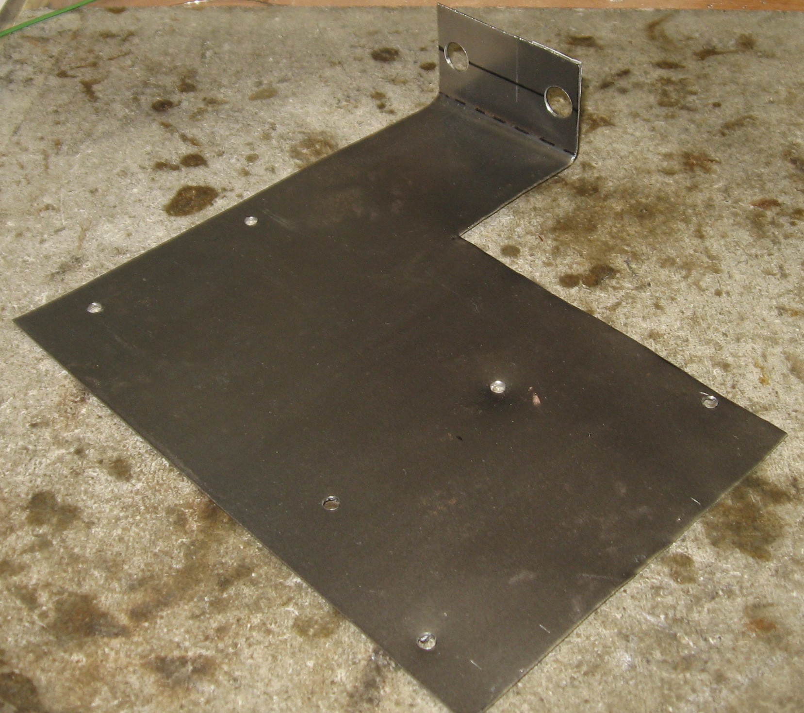
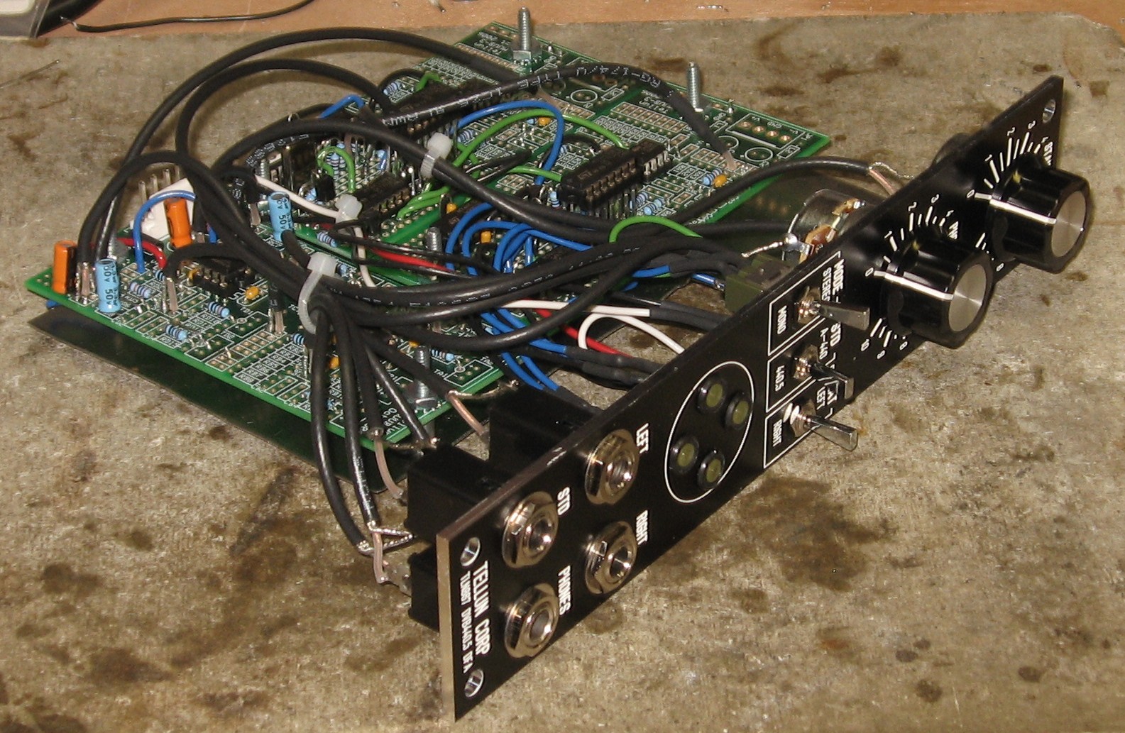
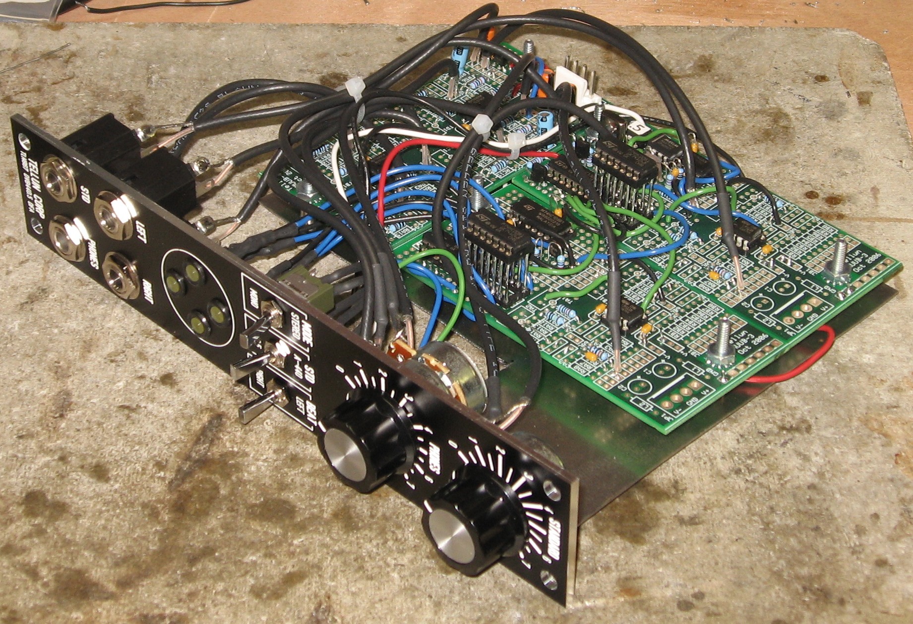
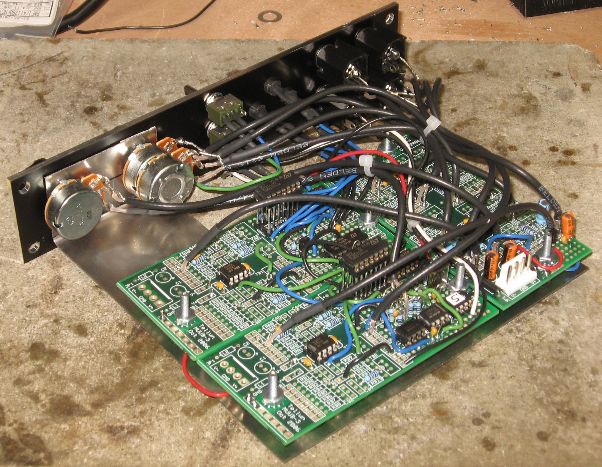
Pre Construction Phase - PCB Mounting Bracket Scott urges assembling the pcb brackets and the panel first. We made a custom mounting bracket. |
||
|
|
||
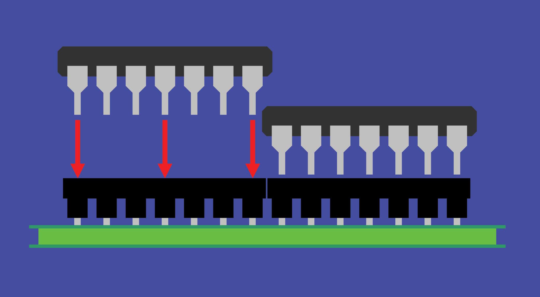
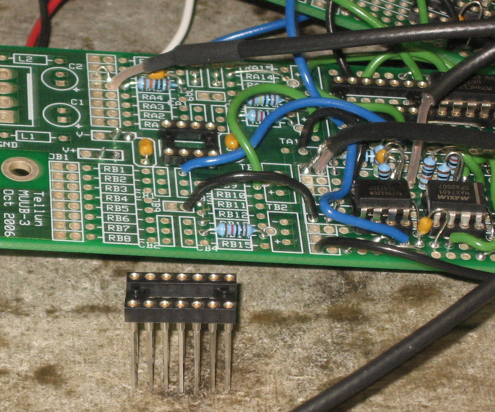
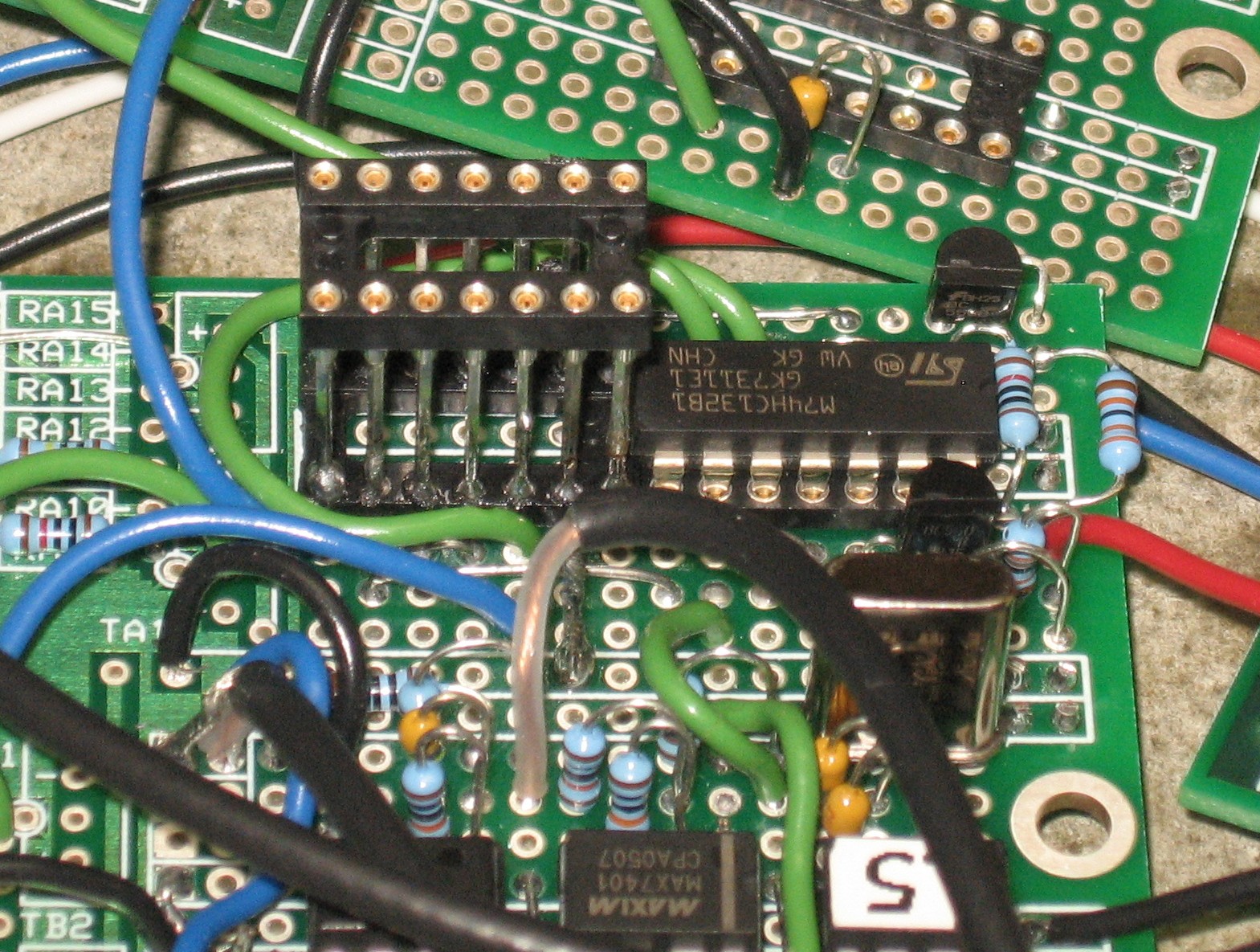
PCBs 2 & 3 IC Physical Conflict Solution.Late in construction when we got to installing the ICs in their sockets, we discovered that the particular ICs we got for U9 and U10 and U12 and U13 wouldn't fit in the contiguous 14-pin sockets provided for them. As a solution, we soldered two long-pinned sockets like this: |
||
|
|
||
Construction / Connections |
||
Go on to Page Two - MUUB ConstructionGo to Page Three - Connections | ||
|
|
||
|
And now, back to work. |
||
Construction Done
|
||
Set up / Testing |
||
Use Notes |
||
|
|
||
|
The fine Print: Use this site at your own risk. We are self-proclaimed idiots and any use of this site and any materials presented herein should be taken with a grain of Kosher salt. If the info is useful - more's the better. Bill and Will © 2005-2011 all frilling rights reserved
|