Bill and Will's Synth
|
||||||||||||||||||||||||||||||||||||||||||||||||||||||||||||||||||||||||||||||||||||||||||||||||||||||||||||||||||||||||||||
Table of Contents |
||||||||||||||||||||||||||||||||||||||||||||||||||||||||||||||||||||||||||||||||||||||||||||||||||||||||||||||||||||||||||||
|
This page has become really long, so here's a table of contents that we hope will make it easier to track: Background - presents an explanation and Jurgen's initial description of the effect Parts - presents a Bill of Materials and notes about it Panel - presents how we came up with our panels' design Construction Phase 1 - Resistors, Capacitors, IC Sockets, Power Plugs, MTA headers Construction Phase 2 - Trimmers - OK, this is where we've left off for now |
||||||||||||||||||||||||||||||||||||||||||||||||||||||||||||||||||||||||||||||||||||||||||||||||||||||||||||||||||||||||||||
Background |
||||||||||||||||||||||||||||||||||||||||||||||||||||||||||||||||||||||||||||||||||||||||||||||||||||||||||||||||||||||||||||
|
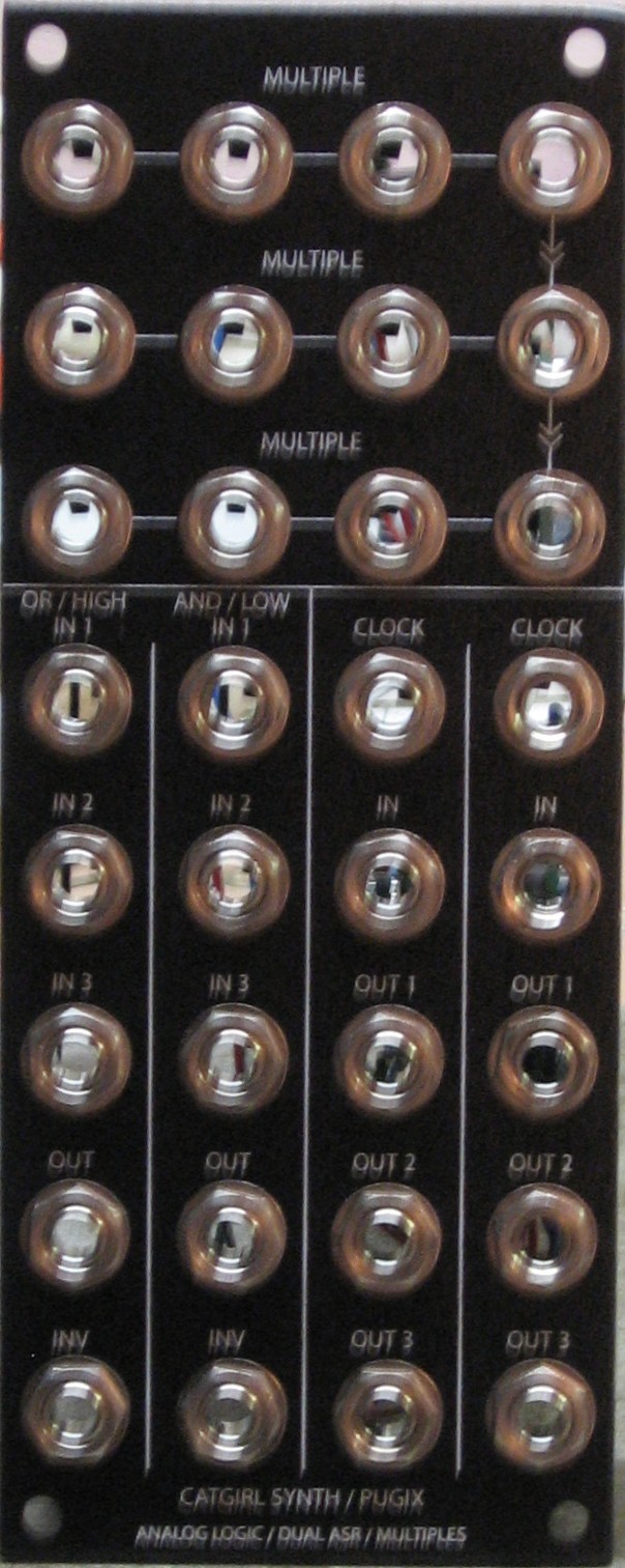
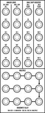
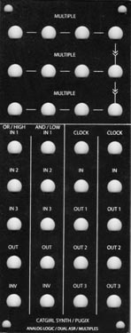
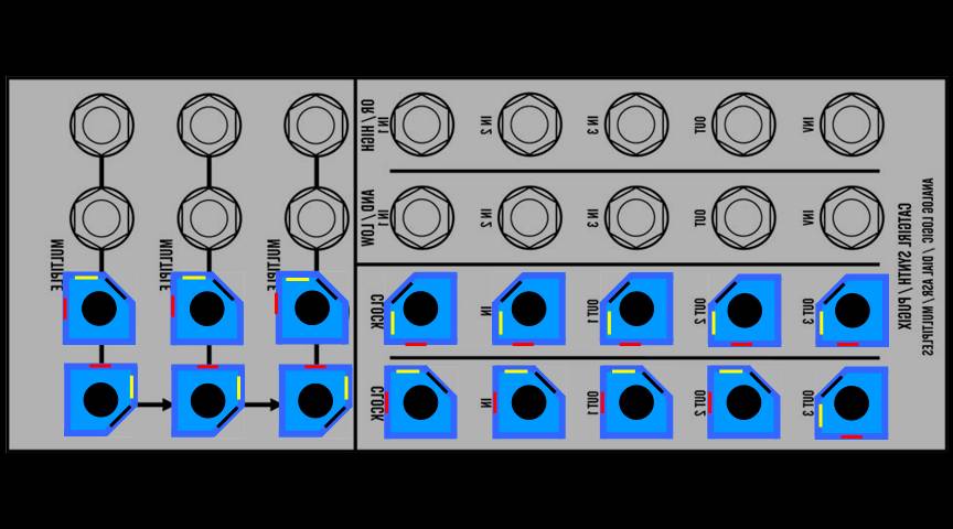
Analog Logic Ken Stone describes the Analog Logic module this way: "This module is the analog implementation of some basic logic elements. Instead of dealing with binary inputs, the "logic" is applied to whatever voltages are present on the inputs. When the AND element is fed several voltages, the output will equal the the lowest input voltage. The NAND output will be the inversion around 0 volts of the AND output. When the OR element is fed several voltages, the output will equal the the highest input voltage. The NOR output will be the inversion around 0 volts of the OR output. Apparently the AND and OR functions are the same thing as "peak" and "trough" on old Serge synthesizers, though they are implemented somewhat differently." The idiot's (our) response: Hunh? - OK - here's how we figured it out: Take a look at the panel. Imitating Richard Brewster, the way we laid it out, the Analog Logic has two columns of five jacks - "OR/HIGH" and "AND/LOW."
We know this is just a re-statement of what Ken says, but it's a little more simply put and therefore easier for us to follow. Shift Register Here's how Ken describes the shift register: "This module is an analog control voltage shift register, three stages in length. It duplicates the functionality of the Serge ASR, but goes about it in a very different way. It is great for producing "arabesque-like" sequences, trills etc., when used with VCOs. Of course it's use is not limited to VCOs only. "Unlike ASRs produced using "bucket brigade" techniques, the CV outputs are constant from the beginning of the cycle to the end - there is no "charge period" in which a brief glide is heard... "...The ASR is nothing more than a 4 stage analog memory. Each cell of this memory is a capacitor, followed by an LF356 buffer. "Addressing each stage of this in turn is half of a 4052 4 pole analog switch. As each cell is addressed, it is forced to follow the incoming voltage. The cell remains connected to the incoming voltage for a full clock cycle, giving it ample time to reach the correct level. "At the same time as this is happening, there are three other 4 pole analog switches that are pointing to each of the other three cells. The first of these points to the cell filled the previous clock cycle, the second to the cycle before than, and the third to the one before that. "As such, once each cell is filled, it remains that way for 3 clock cycles, then is filled with a new voltage on the fourth. The other three cells are cycled in turn to the 1st, 2nd and 3rd outputs." Well - we kinda get it, but how will it actually sound? You know - we're going to have to take this one on faith for a while. It seems like it'll be very interesting - but we don't know how we'll use it yet. Cascading Multiple There are three rows left on the panel where we can put a cascading multiple. Easy! A-la the MOTM-910 only re-arranged a bit on the 2U wide panel. Paul Schrieber describes it (roughly) this way: This is "a passive (needs no power) multiple with..." three "...cascaded 4-way multiples. Switching jacks are used to 'daisy-chain' the..." three "...sections together. Inserting a patch cord in any of..." two "...special locations (indicated by the arrows) breaks the chain... to the mults below. In this manner, you can configure..." it "...many different ways:
|
||||||||||||||||||||||||||||||||||||||||||||||||||||||||||||||||||||||||||||||||||||||||||||||||||||||||||||||||||||||||||||
|
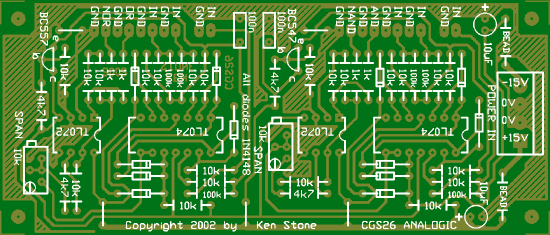
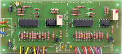
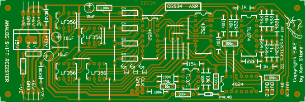
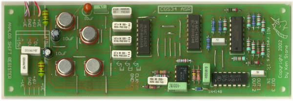
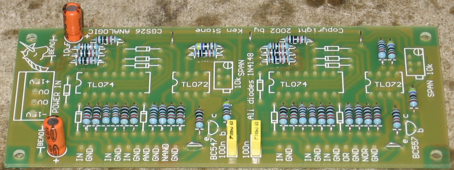
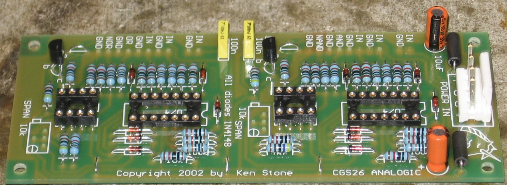
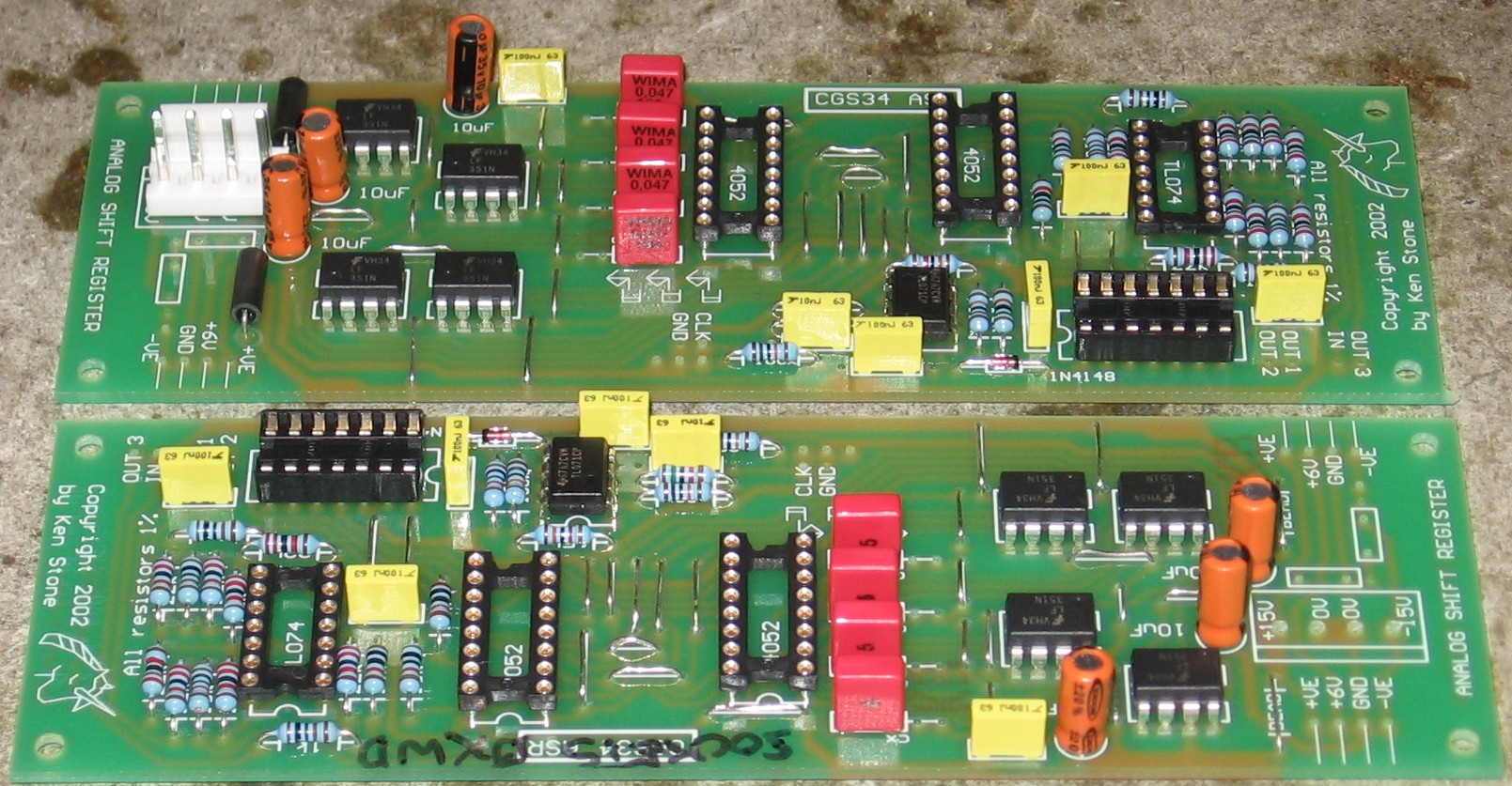
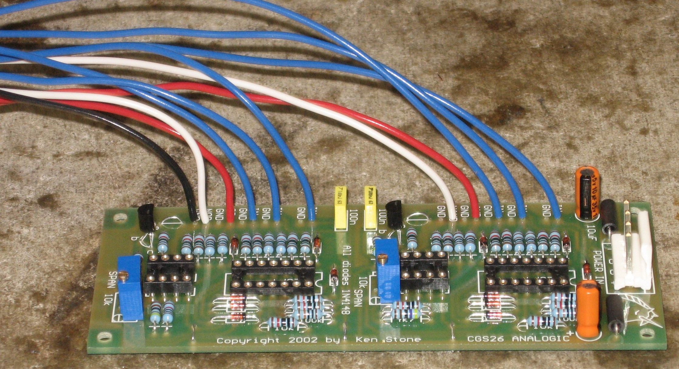
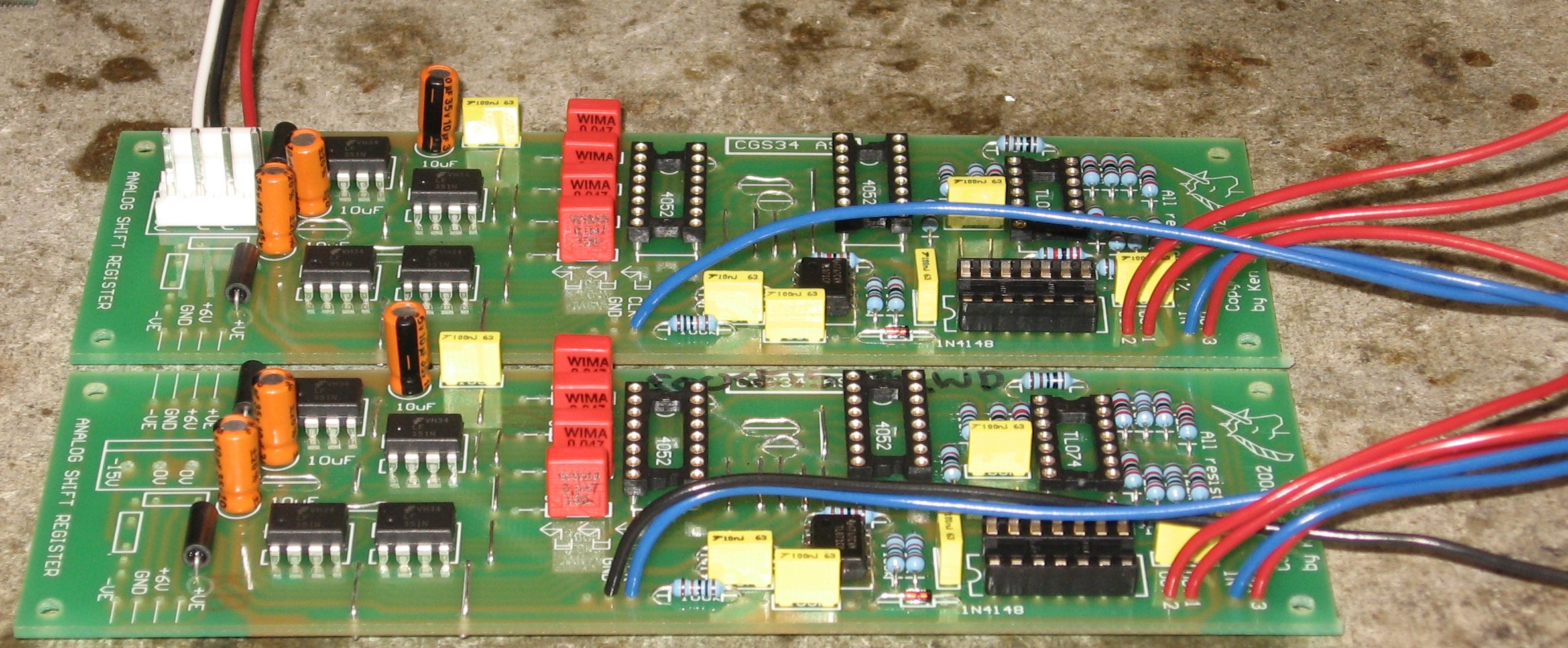
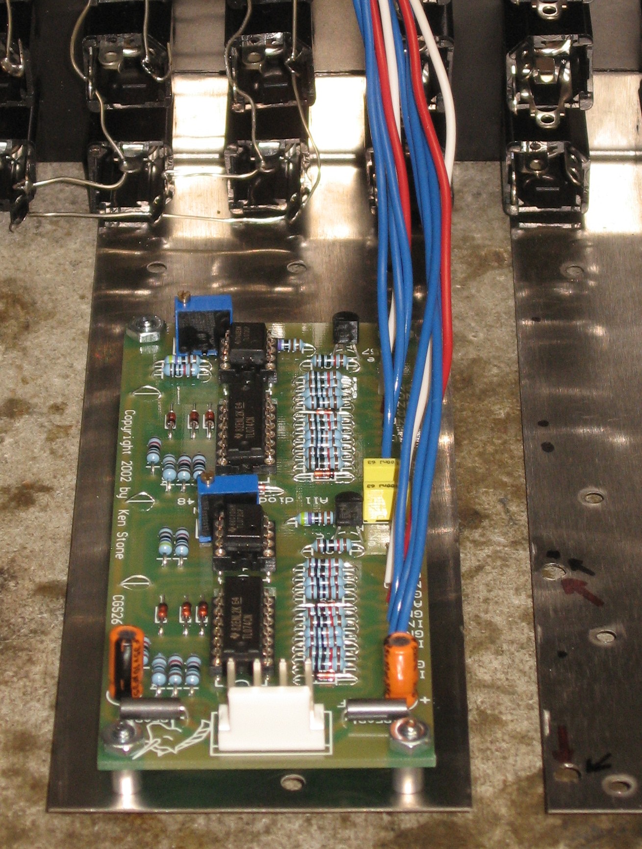
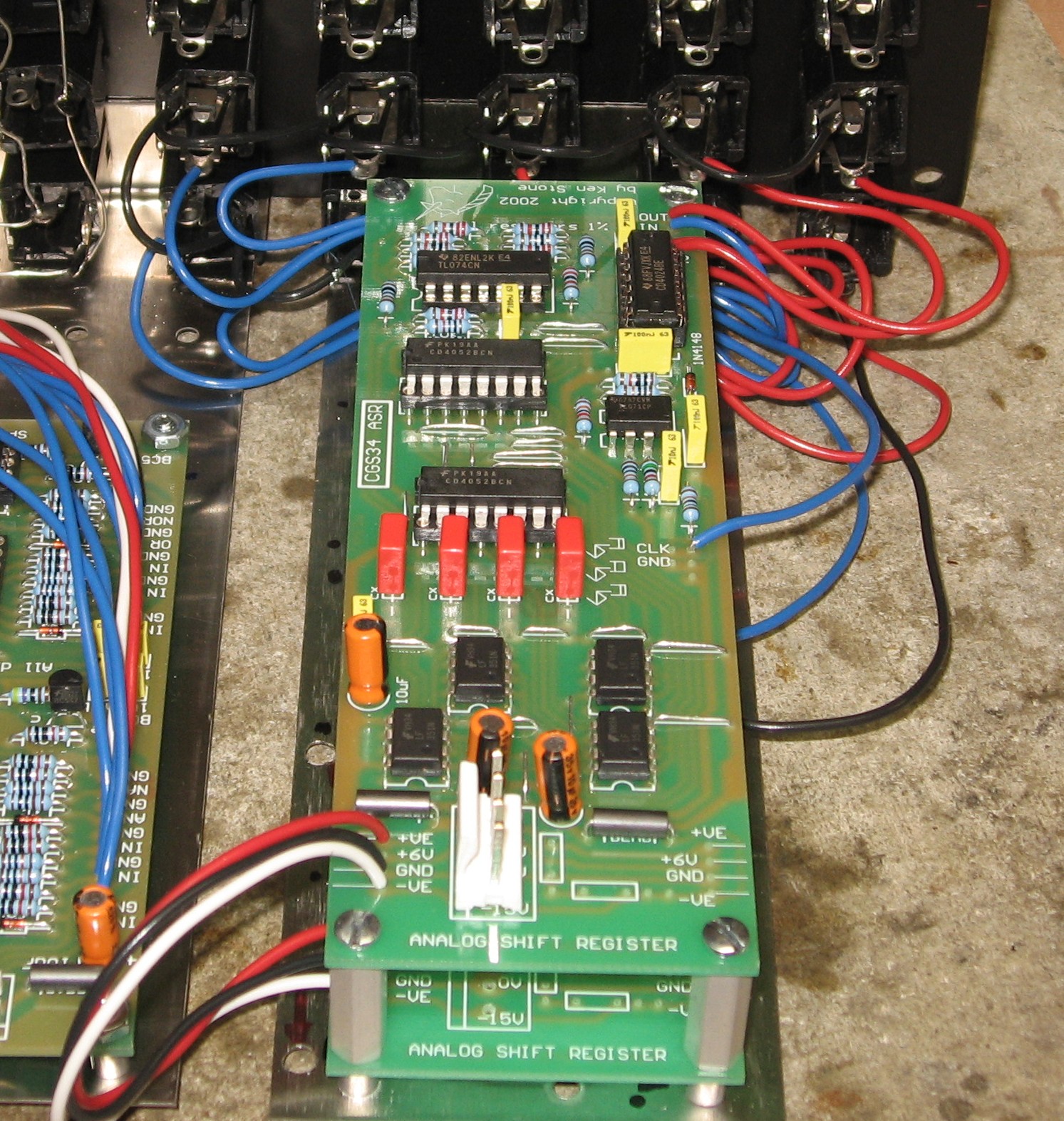
PCBs This module uses three PCBs - One CGS26 Analog Logic PCB, and Two CGS34 Analog Shift Register PCBs. CGS26 Analog Logic PCB
Image courtesy Ken Stone.
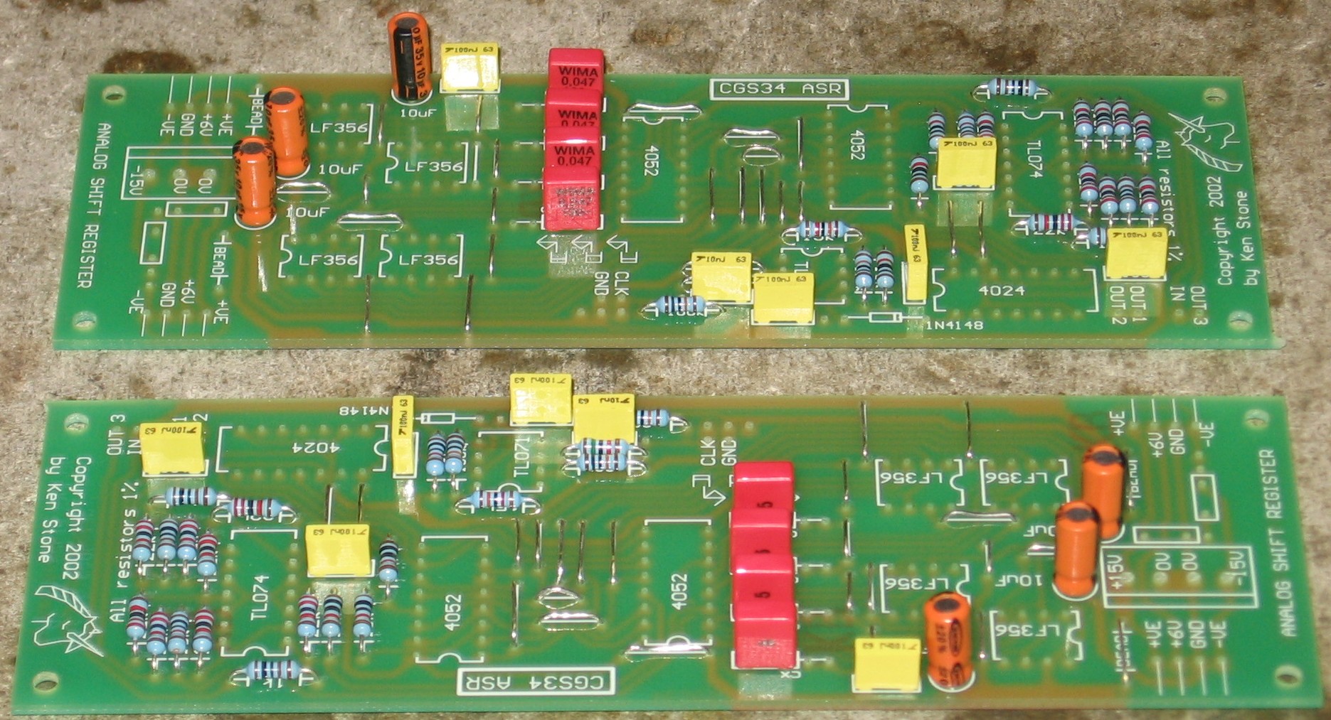
CGS34 Analog Shift Register PCB
Image courtesy Ken Stone.
|
||||||||||||||||||||||||||||||||||||||||||||||||||||||||||||||||||||||||||||||||||||||||||||||||||||||||||||||||||||||||||||
Parts |
||||||||||||||||||||||||||||||||||||||||||||||||||||||||||||||||||||||||||||||||||||||||||||||||||||||||||||||||||||||||||||
|
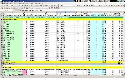
Will and I have developed a parts-list / bill-of-materials in the form of XL spreadsheets. In the BOM, the left-most column is the "part." The parts we've ordered have a green background. These parts we have a high (but not perfect) level of confidence that we've specified correctly. please double-check us and let us know of mistakes you find. CGS26 Analog Logic BOM Corrections to BOM: None yet - Notes: None yet - Click here to download the spreadsheet (apx. 35K). CGS34 Analog Shift Register BOM Note: The CGS34 requires matched diodes for accurate tracking. We'd already measured some and there were 12 diodes that had measured 636 miliVolts - perfect - so we used them. Corrections to BOM: None yet - Notes: None yet - Click here to download the spreadsheet (apx. 35K).
|
||||||||||||||||||||||||||||||||||||||||||||||||||||||||||||||||||||||||||||||||||||||||||||||||||||||||||||||||||||||||||||
Panel |
||||||||||||||||||||||||||||||||||||||||||||||||||||||||||||||||||||||||||||||||||||||||||||||||||||||||||||||||||||||||||||
|
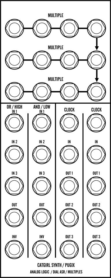
With Richard Brewster's panel design as a starting point, we designed ours to make it clearer for us to use - given our particular eyes. When Scott Deyo at Bridechamber laid the panel out, he put the multiples on top because there wasn't enough room for all the labeling otherwise. No biggie.
|
||||||||||||||||||||||||||||||||||||||||||||||||||||||||||||||||||||||||||||||||||||||||||||||||||||||||||||||||||||||||||||
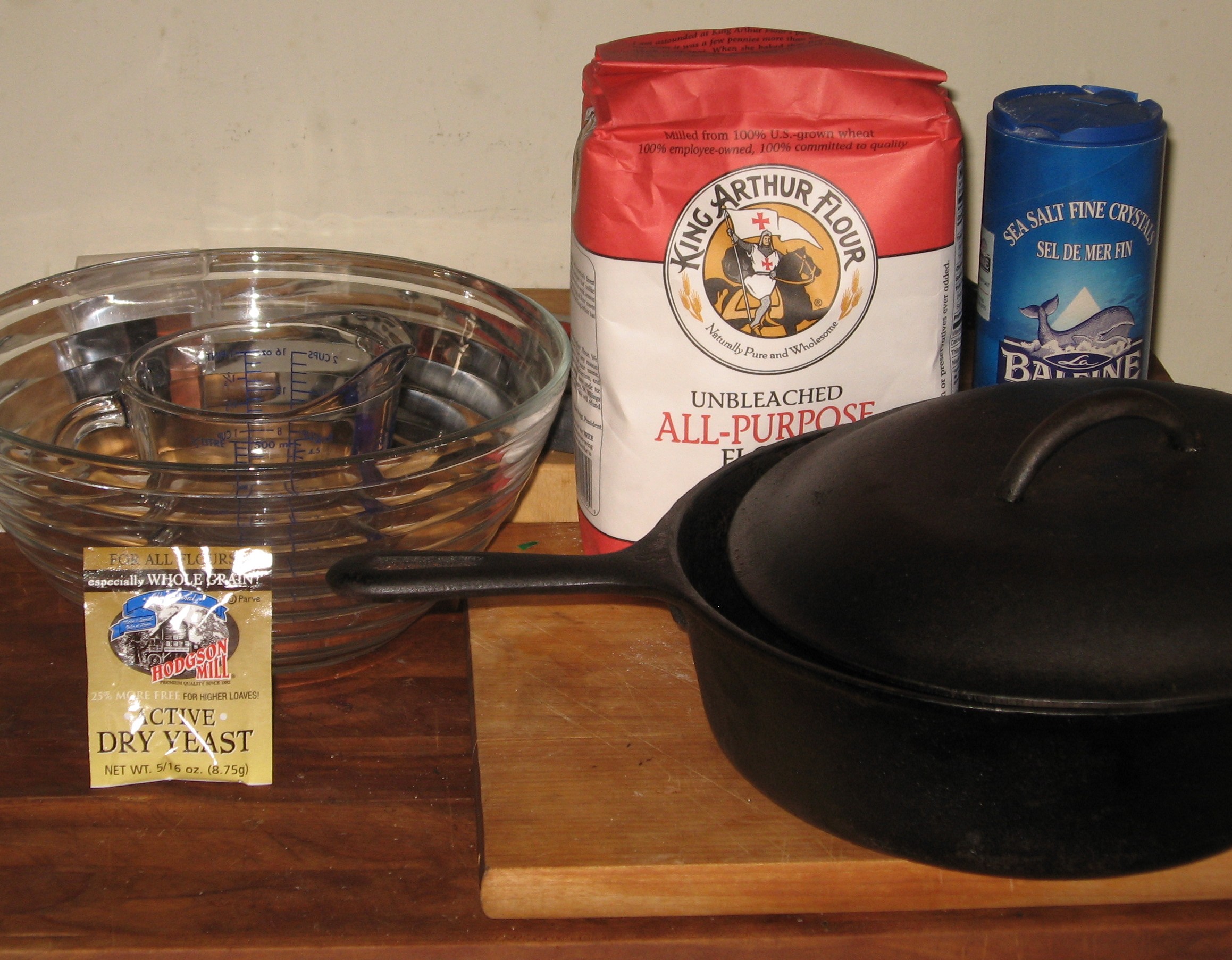
Construction Phase 1All the stuff in Phase 1 gets soldered using "Organic" Solder. At every break in the action, we wash the board off to get rid of the flux. |
||||||||||||||||||||||||||||||||||||||||||||||||||||||||||||||||||||||||||||||||||||||||||||||||||||||||||||||||||||||||||||
|
Jumpers, Resistors, Caps |
||||||||||||||||||||||||||||||||||||||||||||||||||||||||||||||||||||||||||||||||||||||||||||||||||||||||||||||||||||||||||||
|
Our standard resistor orientation rap: whereas we are vigilant about orienting all the resistors, caps, etc. consistently so their values can be read easily (in case we need to trouble-shoot them later), we orient the resistors with the "tolerance" stripe on the left (relative to the text on the PCB). You might want to do it the opposite way - with the "tolerance" stripe on the right - it kinda makes more sense.
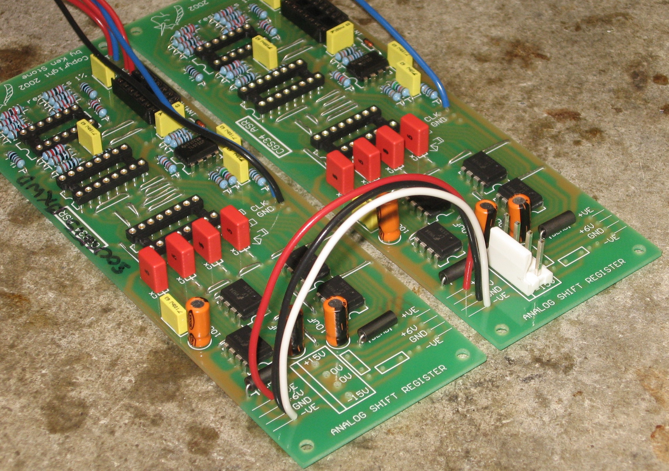
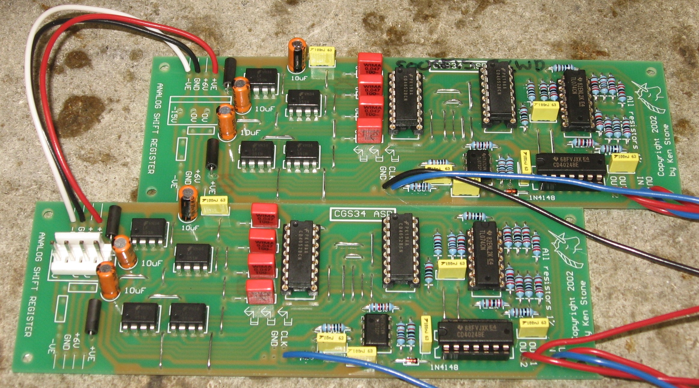
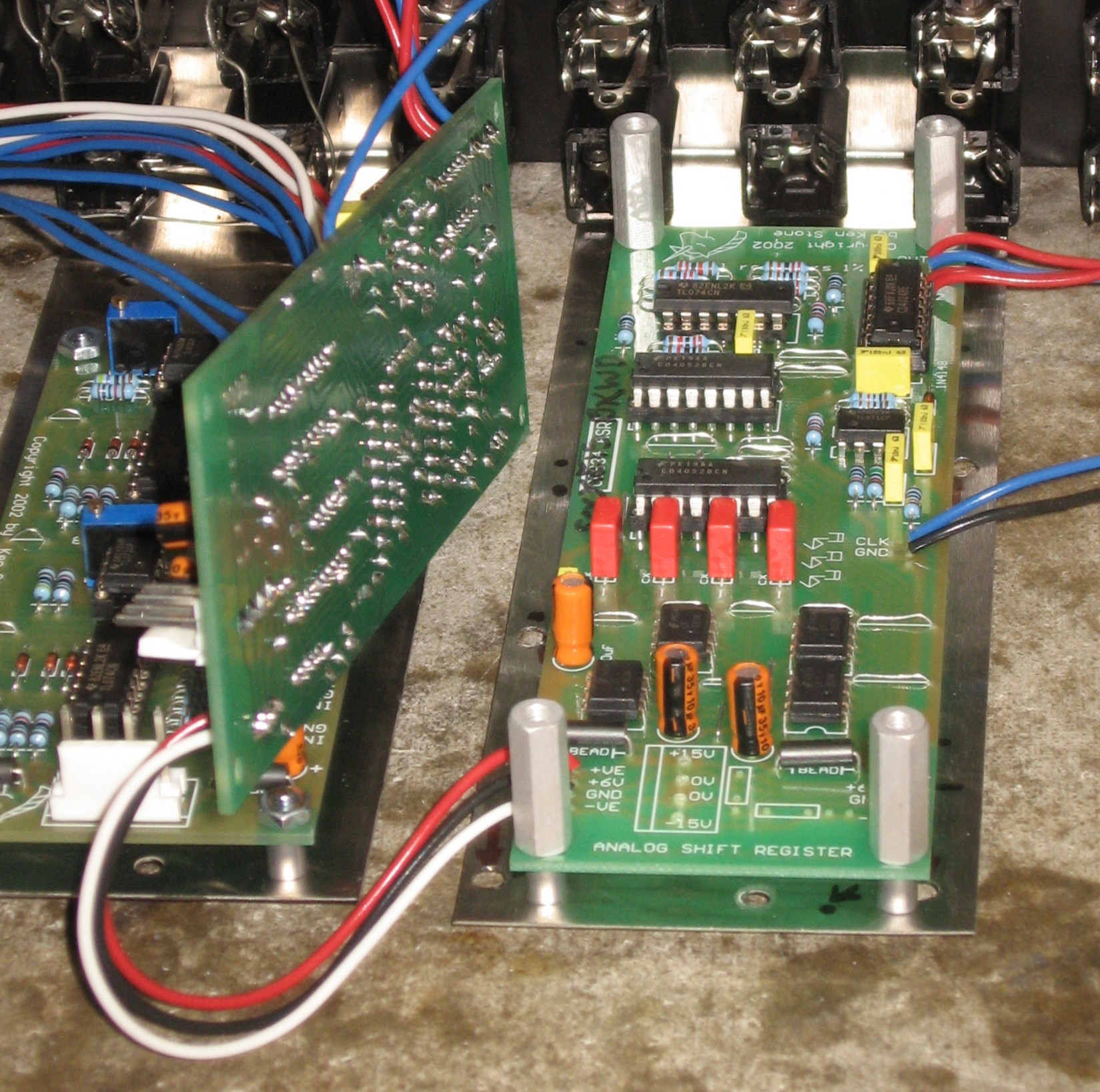
As we were trimming the jumper's leads on one of the GCS34s, we saw what looked like the solder pad shift ever so slightly. So we thought we should test it with an ohm meter. It wasn't "jumping" at that end. And when we tested other ones, we found one other wasn't connected - as if the pad at one end had broken away from the trace. We corrected these by adding a little scrap of resistor lead jumping to the next place along the trace. No prob. When we tested all the other jumpers on the other PCBs, they were fine. Go figure. The two CGS34s are going to be installed one over the other so the power is going to plug into just one of them - the one on top. So at first, we built one of the PCBs (the one that will be underneath the other) with jumpers in place of the Ferrite Beads. But later we found that the way we connected the power from board to board bypassed the ferrite beads so don't build it with jumpers here. Put the ferrite beads in both PCBs. Later on, we changed it and put the ferrite beads in. |
||||||||||||||||||||||||||||||||||||||||||||||||||||||||||||||||||||||||||||||||||||||||||||||||||||||||||||||||||||||||||||
|
Semiconductors, IC Sockets, Power Plugs, etc. |
||||||||||||||||||||||||||||||||||||||||||||||||||||||||||||||||||||||||||||||||||||||||||||||||||||||||||||||||||||||||||||
|
OK - for the CGS34 - some of the holes were too small for our IC sockets. We had these two big, odd, funky ones that had very skinny contacts - we used them for the TL074s. But we ended up soldering the TL071s and the LF356s (that substitute for the LF351s) directly into the PCB. We soldered a couple of the 14-pin sockets in backward and made a note on the PCB ("sockets bkwd") so that we remember to install the IC correctly. Again, the CGS34 requires matched diodes for accurate tracking. We used twelve that we'd already measured to 636 miliVolts.
The power header and ferrite beads solder into the PCB that will be installed on top of the other. |
||||||||||||||||||||||||||||||||||||||||||||||||||||||||||||||||||||||||||||||||||||||||||||||||||||||||||||||||||||||||||||
|
|
||||||||||||||||||||||||||||||||||||||||||||||||||||||||||||||||||||||||||||||||||||||||||||||||||||||||||||||||||||||||||||
Construction Phase 2All the stuff in Phase 2 gets soldered using "No-Clean" Solder and the PCB doesn't get washed off from here on. |
||||||||||||||||||||||||||||||||||||||||||||||||||||||||||||||||||||||||||||||||||||||||||||||||||||||||||||||||||||||||||||
|
Trimmers - for the CGS26 |
||||||||||||||||||||||||||||||||||||||||||||||||||||||||||||||||||||||||||||||||||||||||||||||||||||||||||||||||||||||||||||
|
|
||||||||||||||||||||||||||||||||||||||||||||||||||||||||||||||||||||||||||||||||||||||||||||||||||||||||||||||||||||||||||||
|
PCB / Panel connections |
||||||||||||||||||||||||||||||||||||||||||||||||||||||||||||||||||||||||||||||||||||||||||||||||||||||||||||||||||||||||||||
|
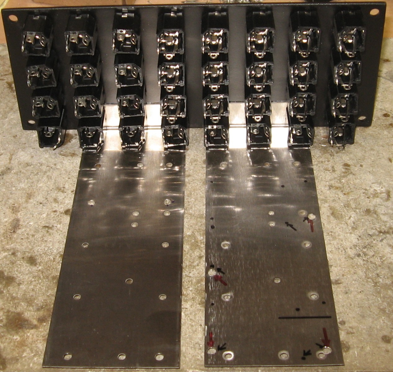
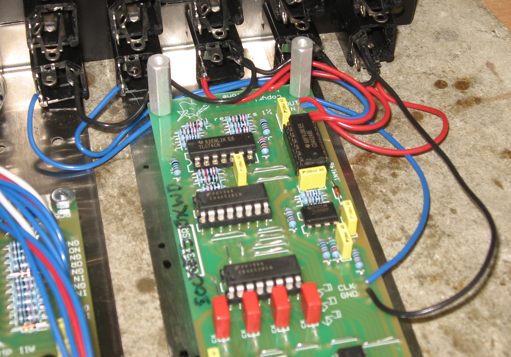
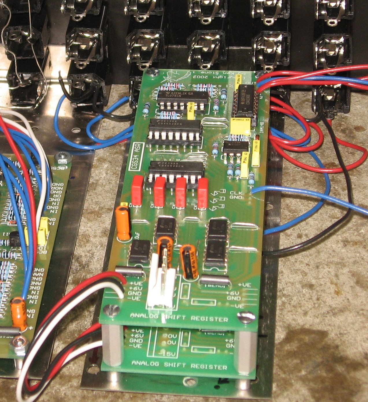
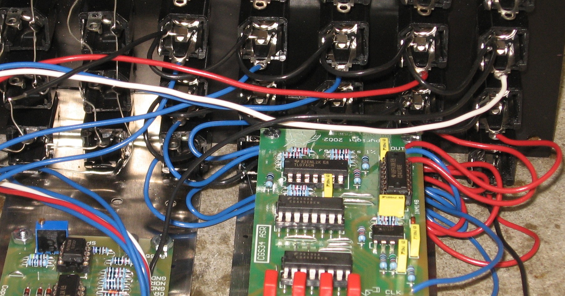
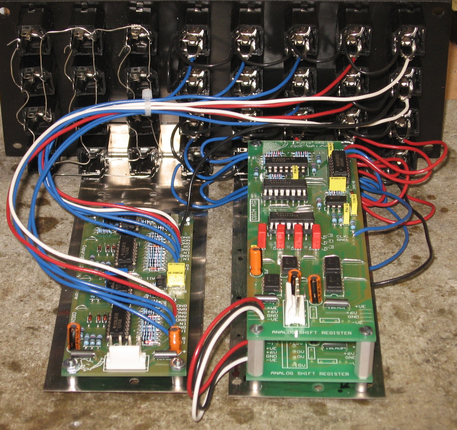
Here's how the PCBs will go on the mounting brackets:
From this, we worked out a chart for the module's connection wiring.
We used only one ground wire to go from the CGS26 PCB and one from the "B" CGS34 to their respective sets of jacks. Then we connected the ground lugs of the jacks together. For this we used twenty-two 1-1/2in pieces of black wire. |
||||||||||||||||||||||||||||||||||||||||||||||||||||||||||||||||||||||||||||||||||||||||||||||||||||||||||||||||||||||||||||
|
Wires Soldered in
|
||||||||||||||||||||||||||||||||||||||||||||||||||||||||||||||||||||||||||||||||||||||||||||||||||||||||||||||||||||||||||||
|
Power from CGS34-A to CGS34-B
|
||||||||||||||||||||||||||||||||||||||||||||||||||||||||||||||||||||||||||||||||||||||||||||||||||||||||||||||||||||||||||||
|
Installing the ICs
|
||||||||||||||||||||||||||||||||||||||||||||||||||||||||||||||||||||||||||||||||||||||||||||||||||||||||||||||||||||||||||||
|
PCB Mounting Brackets |
||||||||||||||||||||||||||||||||||||||||||||||||||||||||||||||||||||||||||||||||||||||||||||||||||||||||||||||||||||||||||||
|
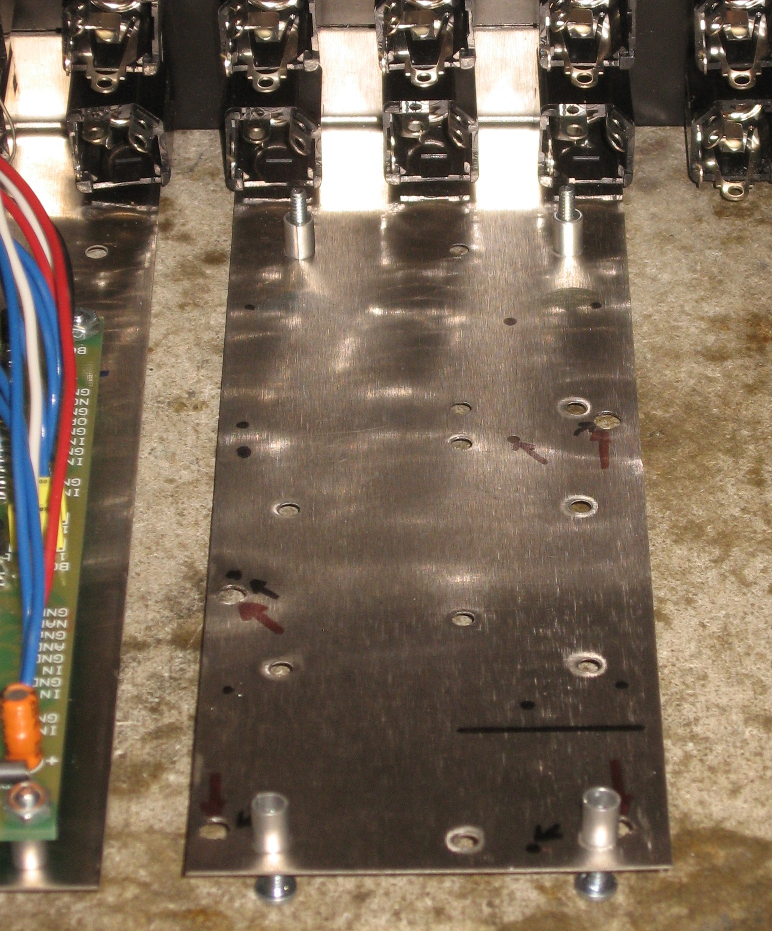
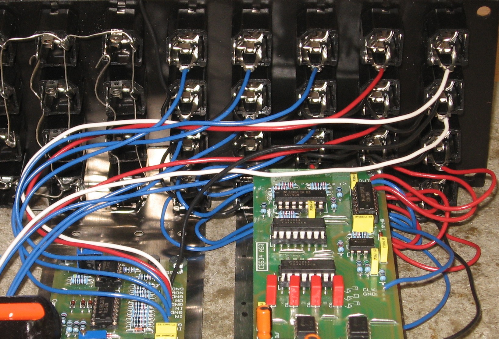
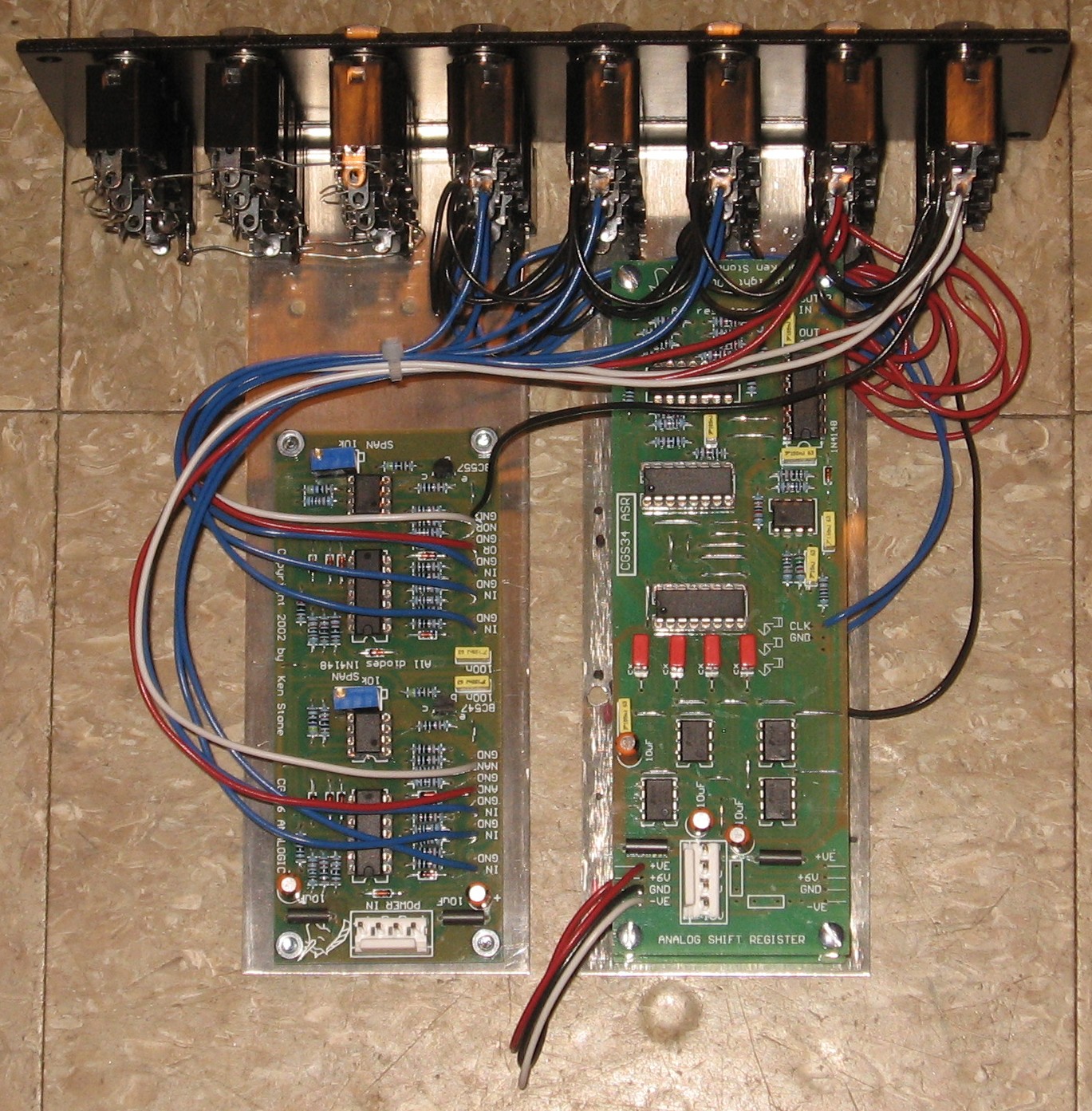
We installed the top-most three rows of jacks in the orientation best for the "multiple" wiring. In the five rows below, we turned the five right-most (from the front) jacks around so that none of the contacts will be too close to the brackets, like this:
Here's how the mounting brackets install - and the jacks:
|
||||||||||||||||||||||||||||||||||||||||||||||||||||||||||||||||||||||||||||||||||||||||||||||||||||||||||||||||||||||||||||
|
Multiples |
||||||||||||||||||||||||||||||||||||||||||||||||||||||||||||||||||||||||||||||||||||||||||||||||||||||||||||||||||||||||||||
|
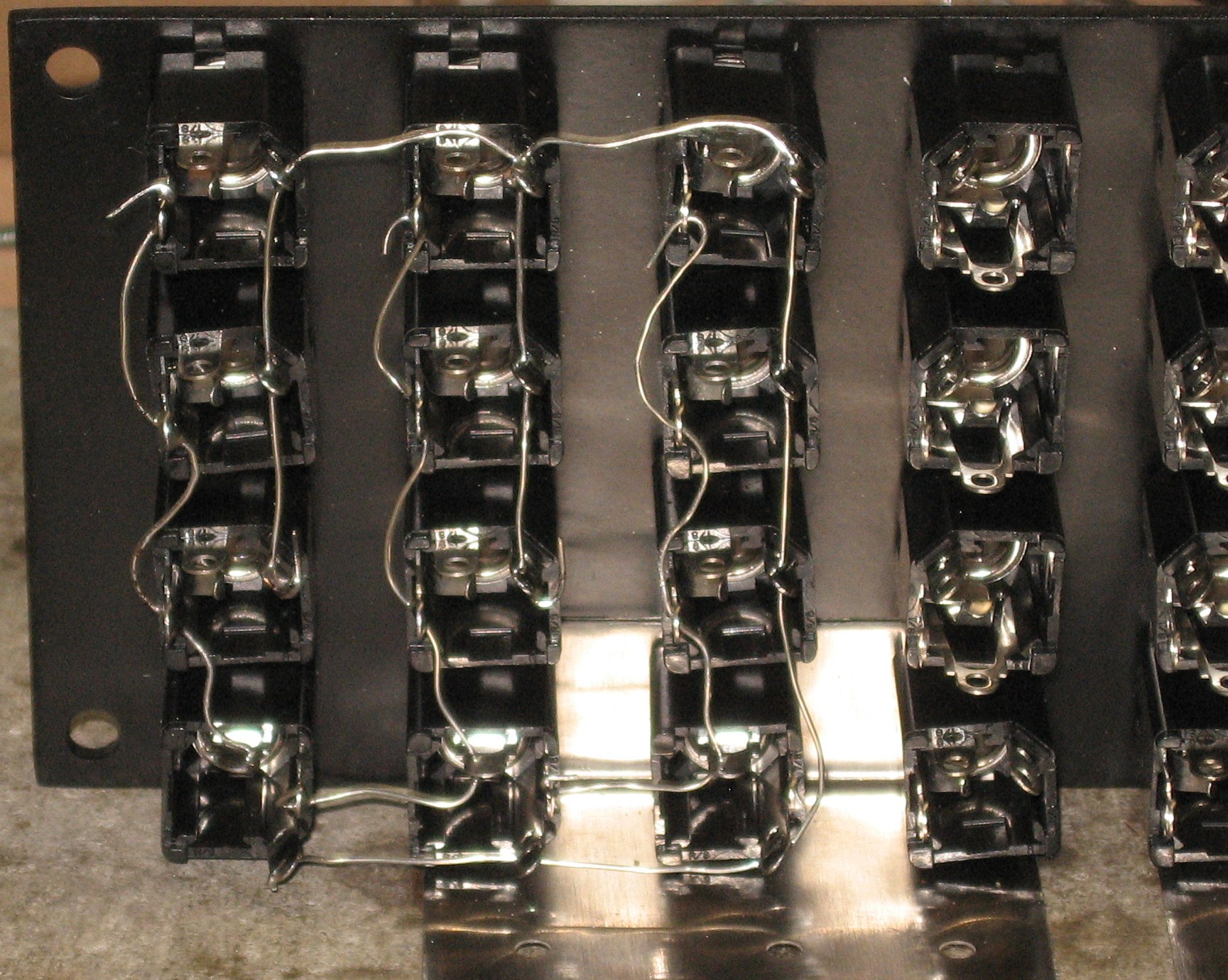
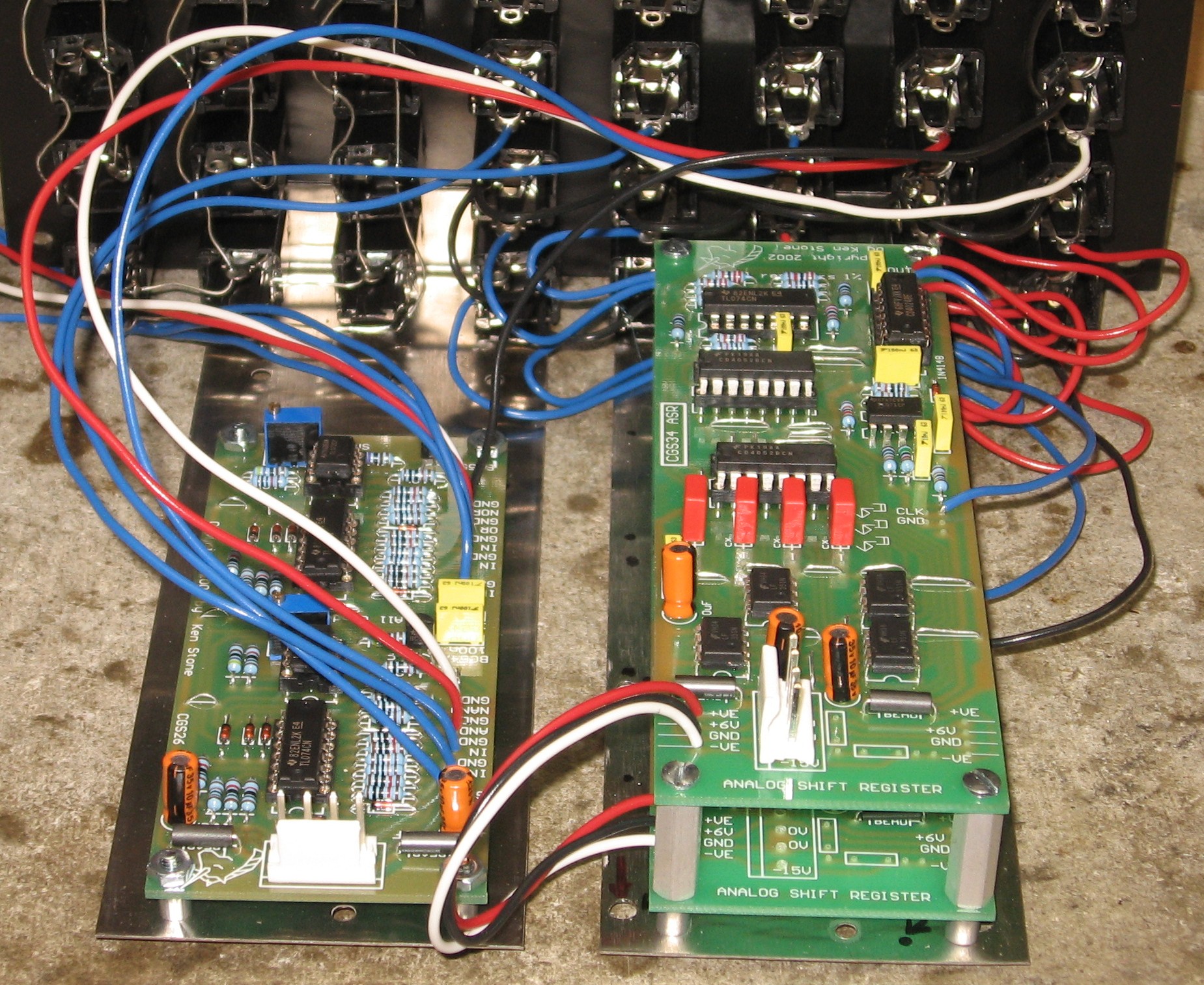
The top-most three rows of jacks are for the multiples. Here's how we wired them up:
|
||||||||||||||||||||||||||||||||||||||||||||||||||||||||||||||||||||||||||||||||||||||||||||||||||||||||||||||||||||||||||||
|
Mounting the CGS26 |
||||||||||||||||||||||||||||||||||||||||||||||||||||||||||||||||||||||||||||||||||||||||||||||||||||||||||||||||||||||||||||
|
|
||||||||||||||||||||||||||||||||||||||||||||||||||||||||||||||||||||||||||||||||||||||||||||||||||||||||||||||||||||||||||||
|
Mounting and Wiring the CGS34s |
||||||||||||||||||||||||||||||||||||||||||||||||||||||||||||||||||||||||||||||||||||||||||||||||||||||||||||||||||||||||||||
|
|
||||||||||||||||||||||||||||||||||||||||||||||||||||||||||||||||||||||||||||||||||||||||||||||||||||||||||||||||||||||||||||
|
Wiring the CGS26 |
||||||||||||||||||||||||||||||||||||||||||||||||||||||||||||||||||||||||||||||||||||||||||||||||||||||||||||||||||||||||||||
|
|
||||||||||||||||||||||||||||||||||||||||||||||||||||||||||||||||||||||||||||||||||||||||||||||||||||||||||||||||||||||||||||
|
Done |
||||||||||||||||||||||||||||||||||||||||||||||||||||||||||||||||||||||||||||||||||||||||||||||||||||||||||||||||||||||||||||
|
|
||||||||||||||||||||||||||||||||||||||||||||||||||||||||||||||||||||||||||||||||||||||||||||||||||||||||||||||||||||||||||||
Set up / Testing |
||||||||||||||||||||||||||||||||||||||||||||||||||||||||||||||||||||||||||||||||||||||||||||||||||||||||||||||||||||||||||||
Use Notes |
||||||||||||||||||||||||||||||||||||||||||||||||||||||||||||||||||||||||||||||||||||||||||||||||||||||||||||||||||||||||||||
|
|
||||||||||||||||||||||||||||||||||||||||||||||||||||||||||||||||||||||||||||||||||||||||||||||||||||||||||||||||||||||||||||


|
The fine Print: Use this site at your own risk. We are self-proclaimed idiots and any use of this site and any materials presented herein should be taken with a grain of Kosher salt. If the info is useful - more's the better. Bill and Will © 2005-2011 all frilling rights reserved
|